Acknowledge, Write data format – Rainbow Electronics MAX9671 User Manual
Page 20
MAX9670/MAX9671
Low-Power Audio/Video Switch with Audio
Volume Control for Dual SCART Connectors
20
______________________________________________________________________________________
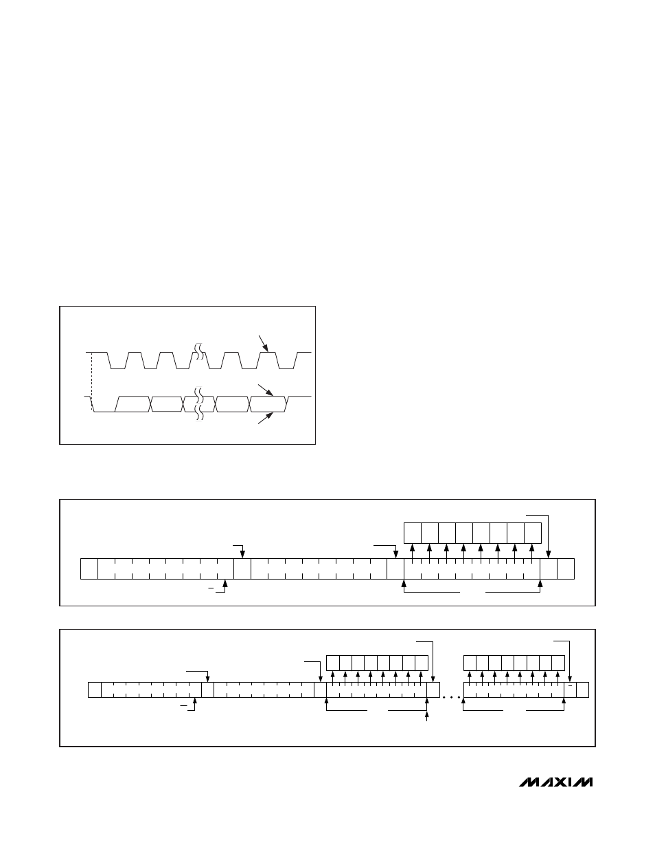
Acknowledge
The acknowledge bit (ACK) is a clocked 9th bit that the
MAX9670/MAX9671 use to handshake receipt of each
byte of data when in write mode (see Figure 8). The
MAX9670/MAX9671 pull down SDA during the entire
master-generated ninth clock pulse if the previous byte
is successfully received. Monitoring ACK allows for
detection of unsuccessful data transfers. An unsuc-
cessful data transfer occurs if a receiving device is
busy or if a system fault has occurred. In the event of
an unsuccessful data transfer, the bus master may retry
communication. The master pulls down SDA during the
ninth clock cycle to acknowledge receipt of data when
the MAX9670/MAX9671 are in read mode. An acknowl-
edge is sent by the master after each read byte to allow
data transfer to continue. A not acknowledge is sent
when the master reads the final byte of data from the
MAX9670/MAX9671, followed by a STOP (P) condition.
Write Data Format
A write to the MAX9670/MAX9671 consists of transmit-
ting a START condition, the slave address with the R/W
bit set to 0, one data byte to configure the internal reg-
ister address pointer, one or more data bytes, and a
STOP condition. Figure 9 illustrates the proper frame
format for writing one byte of data to the
MAX9670/MAX9671. Figure 10 illustrates the frame for-
mat for writing n bytes of data to the MAX9670/
MAX9671.
The slave address with the R/W bit set to 0 indicates
that the master intends to write data to the MAX9670/
MAX9671. The MAX9670/MAX9671 acknowledge
receipt of the address byte during the master-generat-
ed ninth SCL pulse.
The second byte transmitted from the master config-
ures the MAX9670/MAX9671’s internal register address
pointer. The pointer tells the MAX9670/MAX9671 where
to write the next byte of data. An acknowledge pulse is
sent by the MAX9670/MAX9671 upon receipt of the
address pointer data.
1
SCL
START
CONDITION
SDA
2
8
9
CLOCK PULSE FOR
ACKNOWLEDGMENT
ACKNOWLEDGE
NOT ACKNOWLEDGE
Figure 8. Acknowledge
A
0
SLAVE ADDRESS
REGISTER ADDRESS
DATA BYTE
ACKNOWLEDGE FROM MAX9670/MAX9671
R/W
1 BYTE
ACKNOWLEDGE FROM MAX9670/MAX9671
ACKNOWLEDGE FROM MAX9670/MAX9671
B1
B0
B3
B2
B5
B4
B7
B6
S
A
A
P
Figure 9. Writing a Byte of Data to the MAX9670/MAX9671
1 BYTE
AUTOINCREMENT INTERNAL
REGISTER ADDRESS POINTER
ACKNOWLEDGE FROM MAX9670/MAX9671
ACKNOWLEDGE FROM
MAX9670/MAX9671
B1 B0
B3 B2
B5 B4
B7 B6
A
A
0
ACKNOWLEDGE FROM MAX9670/MAX9671
R/W
S
A
1 BYTE
ACKNOWLEDGE FROM
MAX9670/MAX9671
B1 B0
B3 B2
B5 B4
B7 B6
P
A
SLAVE ADDRESS
REGISTER ADDRESS
DATA BYTE 1
DATA BYTE n
Figure 10. Writing n Bytes of Data to the MAX9670/MAX9671