Rainbow Electronics MAX9671 User Manual
Page 18

MAX9670/MAX9671
Low-Power Audio/Video Switch with Audio
Volume Control for Dual SCART Connectors
18
______________________________________________________________________________________
Video Input Control register (06h) while the selection of
video sources that are sent to the VCR SCART connec-
tor are controlled by bits 0 to 2 of the VCR Video Input
Control register (08h). See Tables 10, 14, and 16. The
video outputs can be enabled or disabled by bits 2
through 7 of the Output Enable register (0Dh). See
Table 18.
Slow Switching
The MAX9670/MAX9671 support the IEC 933-1,
Amendment 1, three-level slow switching that selects
the aspect ratio for the display (TV). Under I
2
C control,
the MAX9670/MAX9671 set the slow-switching output
voltage level. Table 2 shows the valid input levels of the
slow-switching signal and the corresponding operating
modes of the display device.
Two bidirectional ports are available for slow-switching
signals for the TV and VCR. The slow-switching input
status is continuously read and stored in the Status reg-
ister (0Eh). The slow-switching outputs can be set to a
logic level or high impedance by writing to the TV Video
Output Control register (07h) and the VCR Video Output
Control register (09h). When enabled, INT becomes
active low if the voltage level changes on TV_SS or
VCR_SS. See Tables 10, 15, 17, and 20.
Fast Switching
The fast-switching signal was originally used to switch
between CVBS and RGB signals on a pixel-by-pixel
basis so that on-screen display (OSD) information
could be inserted. Since modern set-top box decoder
chips have integrated OSD circuitry, there is no need to
create OSD information using the older technique. Now,
the fast-switching signal is just used to switch between
CVBS and RGB signal sources.
Set the source of the fast-switching signal by writing to
bits 4 and 3 of the TV Video Output Control register
(07h). The fast-switching signal to the TV SCART con-
nector can be enabled or disabled by bit 1 of the Output
Enable register (0Dh). See Tables 10, 15, and 18.
I
2
C Serial Interface
The MAX9670/MAX9671 feature an I
2
C/SMBus™-com-
patible, 2-wire serial interface consisting of a serial-data
line (SDA) and a serial-clock line (SCL). SDA and SCL
facilitate communication between the MAX9670/
MAX9671 and the master at clock rates up to 400kHz.
Figure 6 shows the 2-wire interface timing diagram. The
master generates SCL and initiates data transfer on the
bus. A master device writes data to the MAX9670/
MAX9671 by transmitting a START (S) condition, the
proper slave address with the R/W bit set to 0, followed
by the register address and then the data word. Each
transmit sequence is framed by a START and a STOP
(P) condition. Each word transmitted to the
MAX9670/MAX9671 is 8 bits long and is followed by an
acknowledge clock pulse. A master reads from the
MAX9670/MAX9671 by transmitting the slave address
with the R/W bit set to 0, the register address of the reg-
ister to be read, a REPEATED START (Sr) condition, the
slave address with the R/W bit set to 1, followed by a
series of SCL pulses. The MAX9670/MAX9671 transmit
data on SDA in sync with the master-generated SCL
pulses. The master acknowledges receipt of each byte
of data. Each read sequence is framed by a START or
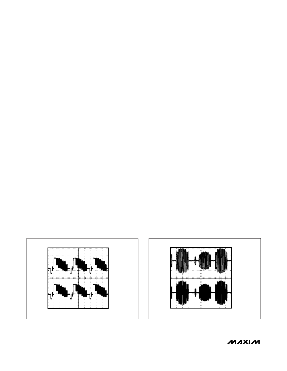
MAX9670 fig04
20
µs/div
INPUT
500mV/div
OUTPUT
500mV/div
Figure 4. MAX9670/MAX9671 Video Output with CVBS Signal,
Multiburst Video Test Signal Shown
MAX9670 fig05
10
µs/div
INPUT
200mV/div
OUTPUT
200mV/div
Figure 5. MAX9670/MAX9671 Video Output with Chroma (C)
Signal, Multiburst Video Test Signal Shown
