System unit components, 2 system unit components, 1 hardware overview 1.2 system unit block diagram – Toshiba TECRA S1 User Manual
Page 20: Figure 1-3 is a block diagram of the system unit, Figure 1-3 system unit block diagram, 6 tecra s1 maintenance manual
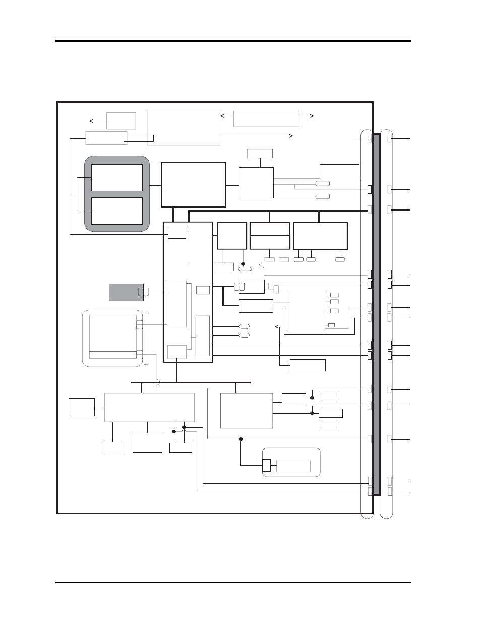
1 Hardware Overview
1.2 System Unit Block Diagram
1-6
TECRA S1 Maintenance Manual
1.2 System Unit Components
Figure 1-3 is a block diagram of the system unit.
PC 2100 DRAM
133MHz
ADM1032
(Thermal Sensor)
MAX6501
CPU : Intel
Mobile
Banias
1.4, 1.5, 1.6, 1.7GM2
Micro FC.PGA2
Main CLK General.
(ICS950810)
LM2729
CPUVID
AGP
32MB
ATI
M9P
LVDS
LCD 14", 15"
CRT
MCH-M
North Bridge
855PM(ODEM)
DC
Expansion
Memory
128/256/512
Expansion
Memory
128/256/512
P
SM
Bus
Cont.
South Bridge
(ICH4-M)
IDE
Cont.
AC97
USB
Cont.
(02)
PCI-PC
Bridge
HUB
Link
Internal PCI Bus
LAN
Cont.
82562
Mini
PCI Slot
802.11b or
Combo
(Wireless LAN)
Cardbus Controller
CB720
EEPROM
MDC
Modem
Int-HDD
30-80GB
9.5mm
Speaker
x2
Line out
Mic
Line in
Antena
PCMCIA
SD
HP
USB
FDD
CODEC
AD1886
AMP
(LM4873)
AC
USB Port
BT
USB P0-P2
USB P3
USB P4
USB P5
USB
USB
2nd HDD
CD-ROM
DVD-ROM
CD-R/RW
Multi Driver
(LS 120)
(ZIP 250)
2nd BATTERY
NTSC/PAL
Serial
Parallel
FIR
DR/RCV
(MAX3243)
(2/2) Super I/O
(LPC47N253)
Internal LPC
Main Battery
E2PROM
I2C
I2C
(1/2) EC/KBC
(LPC 47N253)
Flash
ROM
K/B
Touch
Pad
PS/2
PS/2
PS/2
RJ45
RJ11
Figure 1-3 System unit block diagram