Functional overview – Renesas M3A-HS60 User Manual
Page 19
Functional Overview
2.3.2 Flash Memory M5M29KT331AVP (included as standard equipment)
Rev.1.00 June 1,2005
2-5
REJ11J0002-0100Z
2
Table2.3.2 Examples for Bus State Controller Settings (Flash Memory Write/Read)
User Area
Applicable Device
Bus State Controller Settings
CS0
M5M29KT331AVP
CS0 Space Bus Control Register : CS0BCR
Initial value : H'36DB 0600(when MD2= H and MD0=L)
Recommended set value : H'1000 0400
• Specify idle state in write to read and write to write intervals
IWW[2:0] = B'001: 1 idle cycles inserted
• Specify data bus
BSZ[1:0] = B'10 : 16-bit bus width
CS0 Space Wait Control Register (CS0WCR)
Initial value: H'0000 0500
Recommended set value : H'0000 0AC1
• Address, CS0# assert -> RD#, WEn# assert delay cycle
SW[1:0] = B'01 : 1.5 cycles
• Specify access wait cycles
WR[3:0] = B'0110 : 5 cycles
• RD#, WEn# negate -> Address, CS0 negate delay cycle
HW[1:0] = B'01 : 1.5 cycles
Write1
Write2
Read1
DATA
DATA
DATA
tDF(OE)
ta(CE1)
ta(AD)
ta(OE)
tWDH1
tWDD1
tWDH1
tWDD1
tWED1
tWED1
tWED1
tWED1
tRSD
tRSD
tCSD1
tCSD1
tCSD1
tCSD1
tCSD1
tCSD1
tAD1
tAD1
tAD1
tAD1
tAD1
tAD1
tRDH1
tRDS1
tDH
tDS
tDH
tDS
tOEH
tAH
tAS
tCH
tWP
tWPH
tWP
tAH
tAS
tWPH
tCH
tWP
tCS
tWP
tRC
tRC
tWC
tWC
T1
T2
Tw4
T1
Tw1
Tw2
Tw1
Tw2
T2
T1
Tw1
Tw2
Tw3
T2
Tf
Tf
Taw1
Taw1
Th
Th
Th
Tf
Tw4
Tw3
Tw3
Tw4
Tw5
Tw5
Tw5
CKIO
A21-A1
CS0#
RD#
WE0#
D15-D0
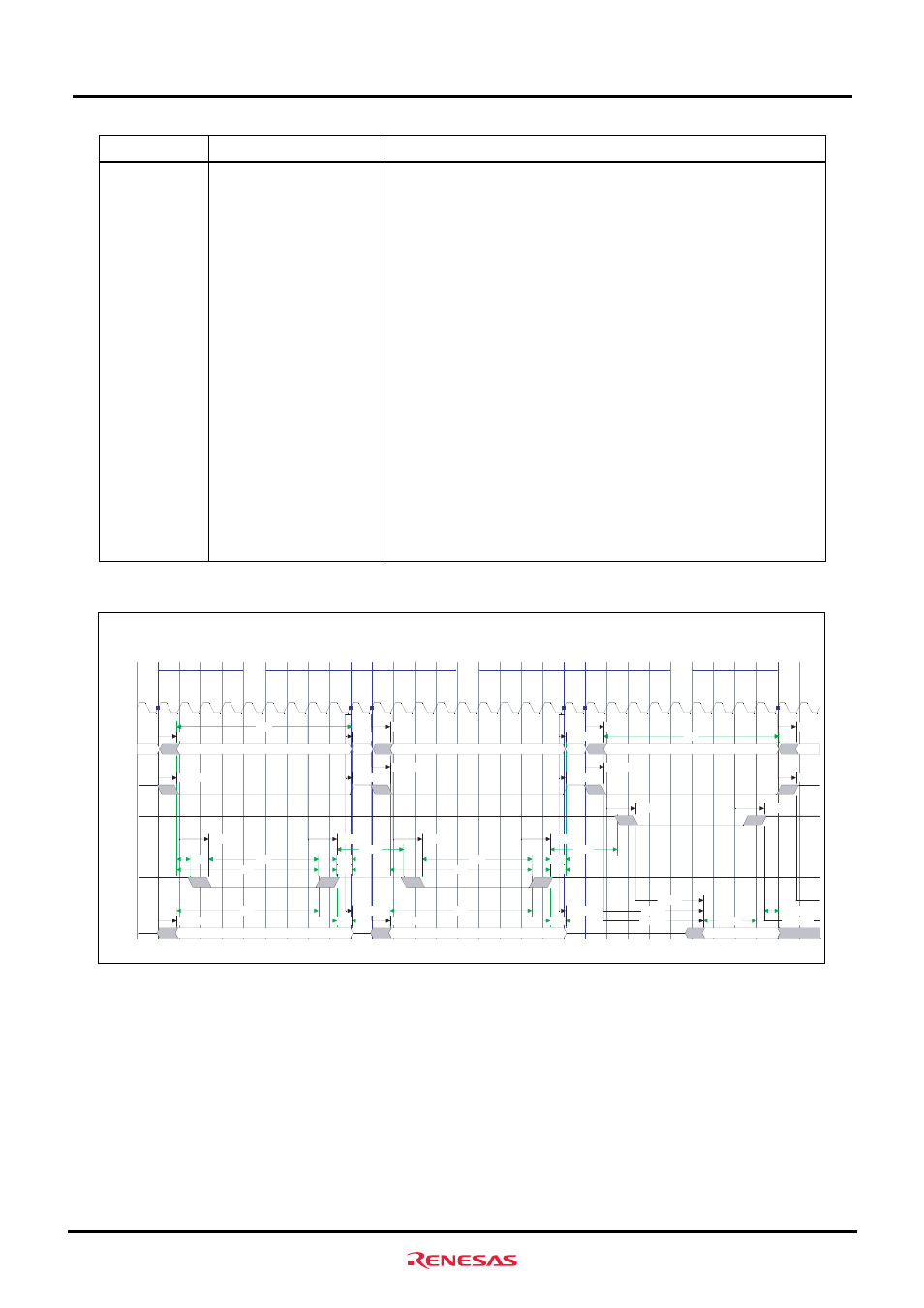
Figure2.3.2 Flash Memory Read and Write Access Timing