7 m3a-hs60 memory mapping – Renesas M3A-HS60 User Manual
Page 12
Overview
1.7 M3A-HS60 Memory Mapping
Rev.1.00 June 1,2005
1-8
REJ11J0002-0100Z
1
1.7 M3A-HS60 Memory Mapping
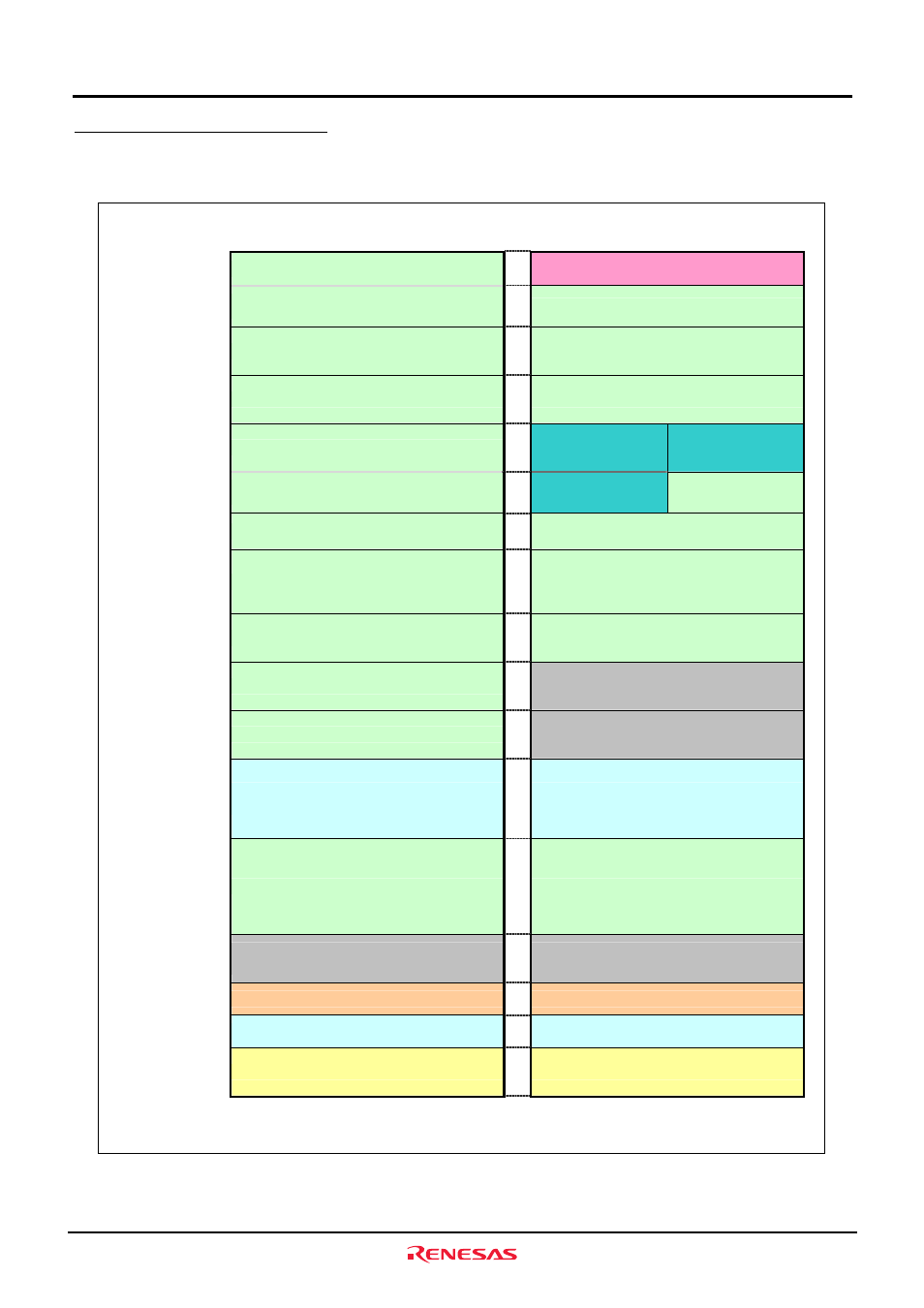
Figure1.7.1 shows the memory mapping example of SH7206 in the M3A-HS60.
Logical address
Logical space of theSH7206
Memory Mapping of theM3A-HS60
H'0000 0000
H'003F FFFF
CS0 space:64MB
Flash Memory(4MB)
16-bit bus
User area
H'0400 0000
CS1 space:64MB
User area
H'0800 0000
CS2 space:64MB
User area
H'0C00 0000
H'0CFF FFFF
CS3 space:64MB
SDRAM(32MB)
32-bit bus
SDRAM(16MB)
16-bit bus
H'0DFF FFFF
User area
User area
H'1000 0000
CS4 space:64MB
User area
H'1400 0000
CS5 space:64MB
User area
H'1800 0000
CS6 space:64MB
Reserved area
(Disabled)
H'1C00 0000
CS7 space:64MB
Reserved area
(Disabled)
H'2000 0000
CS0-CS7 spaces
(non-cacheable area)
CS0-CS7 spaces
(non-cacheable area)
H'4000 0000
CS8 space:1GB
User area
H'8000 0000
Reserved area
(Disabled)
Reserved area
(Disabled)
H'FFF8 0000
Internal RAM(128KB)
Internal RAM(128KB)
H'FFFA 0000
Internal RAM, Reserved
Internal RAM, Reserved
H'FFFC 0000
H'FFFF FFFF
Internal peripheral module
Internal peripheral module
Note: There is the cacheable area from H’0000 0000~H’1FFF FFFF.
Figure1.7.1 Memory Mapping Example of SH7206