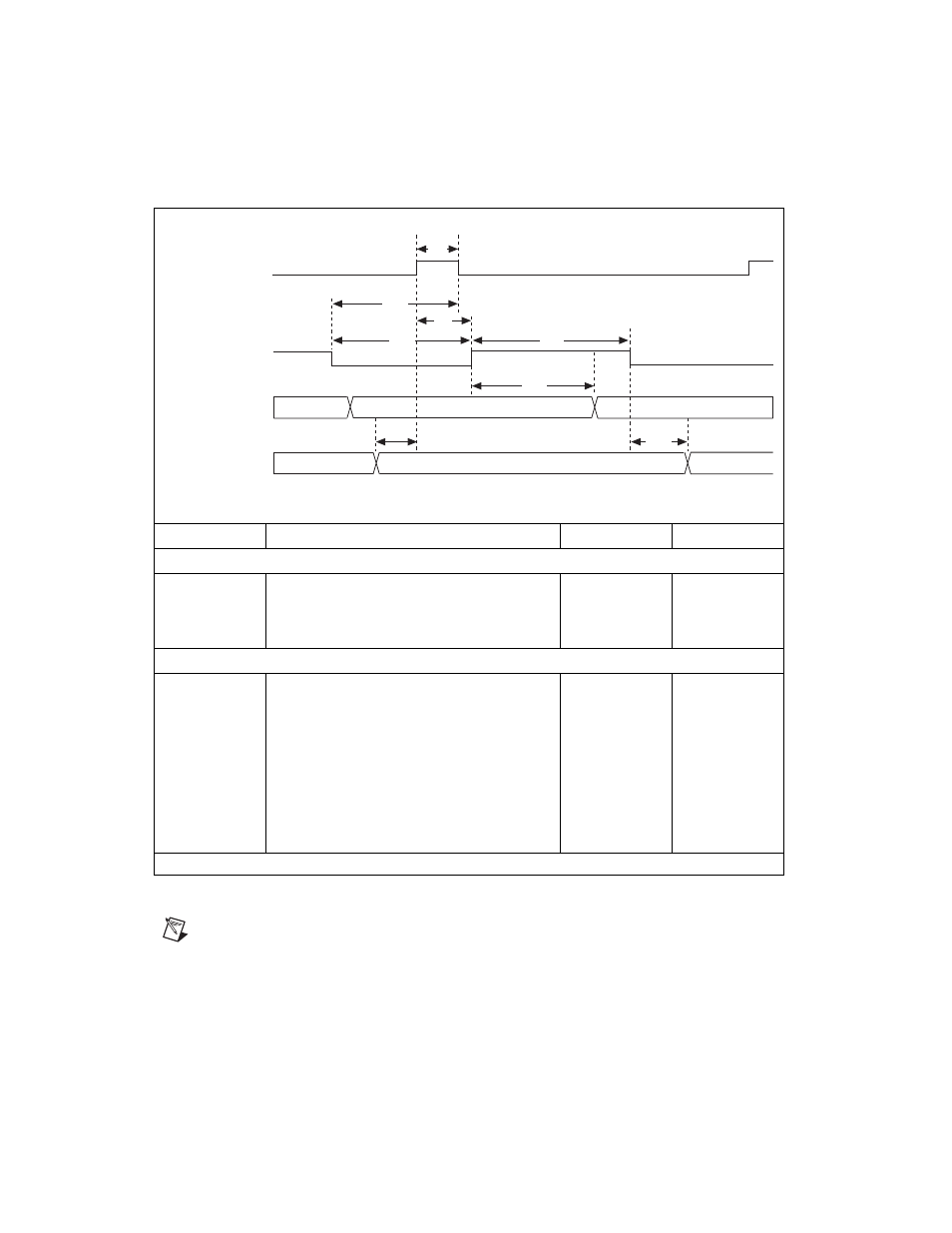
Figure 3-31. leading edge output timing diagram – National Instruments 653X User Manual
Page 85

Chapter 3
Timing Diagrams
3-34
ni.com
Figure 3-31. Leading Edge Output Timing Diagram
Note
With REQ edge latching disabled (default), output data valid will hold t
rdo
ns after
the REQ edge occurs. With REQ edge latching enabled, that data will be held for at most
t
rdo
ns after the REQ edge deasserts.
Parameter
Description
Minimum
Maximum
Input Parameters
t
rr*
REQ pulse width
75
—
t
r*r
REQ inactive duration
75
—
t
ar
ACK to next REQ
0
—
Output Parameters
t
aa*
ACK pulse width
125
—
t
r*a*
REQ inactive to ACK inactive
150
—
t
r*do
REQ inactive to new output data
(with REQ-edge latching)
0
50
t
rdo
REQ to new output data
(with REQ-edge latching disabled)
0
—
t
doa
Output data valid to ACK
(with REQ-edge latching disabled)
25
1
—
1
t
doa
(min.) = 25 + programmable delay
REQ
Output Data Valid
(REQ-edge
latching)
Output Data Valid
(REQ-edge
latching disabled)
t
r*r
t
r*a*
t
r*do
t
doa
t
ar
t
aa*
t
rr*
ACK
t
rdo
ACK and REQ are shown as active high
