Datasheet – SMSC USB2640i User Manual
Page 20
Ultra Fast USB 2.0 Multi-Format Flash Media Controller/USB Hub Combo
Revision 2.0 (10-03-08)
20
SMSC USB2640/USB2641
DATASHEET
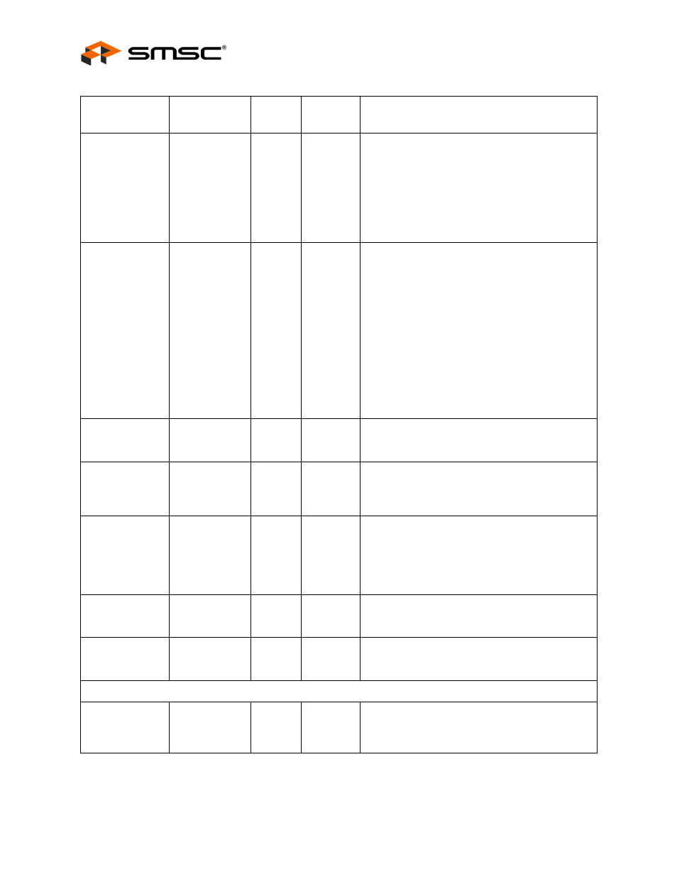
USB Power
Enable
PRTCTL[3:2]
7
6
I/OD12PU
As an output, these pins enables power
downstream USB peripheral devices. See
for diagram and usage
instructions.
As an input, when the power is enabled, these
pins monitor the over-current condition. When an
over-current condition is detected, the pins turn the
power off.
Detect Upstream
VBUS Power
VBUS_DET
39
I
Detects the state of upstream VBUS power. The
Hub monitors VBUS_DET to determine when to
assert the internal D+ pull-up resistor (signaling a
connect event).
When designing a detachable hub, connect this
pin to the VBUS power pin of the USB port that is
upstream of the Hub.
For self-powered applications with a permanently
attached host, this pin should be pulled up,
typically to VDD33.
VBUS is a 3.3V input. A resistor divider must be
used when connecting to 5V USB power.
USB Transceiver
Bias
RBIAS
47
I-R
A 12.0 k
Ω
,
±
1.0% resistor is attached from VSSA
to this pin in order to set the transceiver's internal
bias currents.
Crystal
Input/External
Clock Input
XTAL1
(CLKIN)
45
ICLKx
24 MHz Crystal or external clock input.
This pin can be connected to one terminal of the
crystal or it can be connected to an external
24MHz clock when a crystal is not used.
Crystal
Output
XTAL2
44
OCLKx
24 MHz Crystal.
This is the other terminal of the crystal, or it is left
open when an external clock source is used to
drive XTAL1(CLKIN).
Note:
Do not use it to drive any external
circuitry other than the crystal circuit.
1.8V PLL Power
Bypass
VDD18PLL
46
This pin is the 1.8V Power bypass for the PLL.
This requires an external bypass capacitor of 1.0
μF minimum.
3.3V Analog
Power
VDDA33
5
41
48
3.3V Analog Power
SPI INTERFACE
SPI Chip Enable
SPI_CE_N
8
O12
This is the active low chip enable output.
If the SPI interface is enabled, this pin must be
driven high in power down states.
Table 6.1 USB2640/USB2641 Pin Descriptions (continued)
NAME
SYMBOL
48-PIN
QFN
BUFFER
TYPE
DESCRIPTION