Datasheet – SMSC USB2640i User Manual
Page 19
Ultra Fast USB 2.0 Multi-Format Flash Media Controller/USB Hub Combo
SMSC USB2640/USB2641
19
Revision 2.0 (10-03-08)
DATASHEET
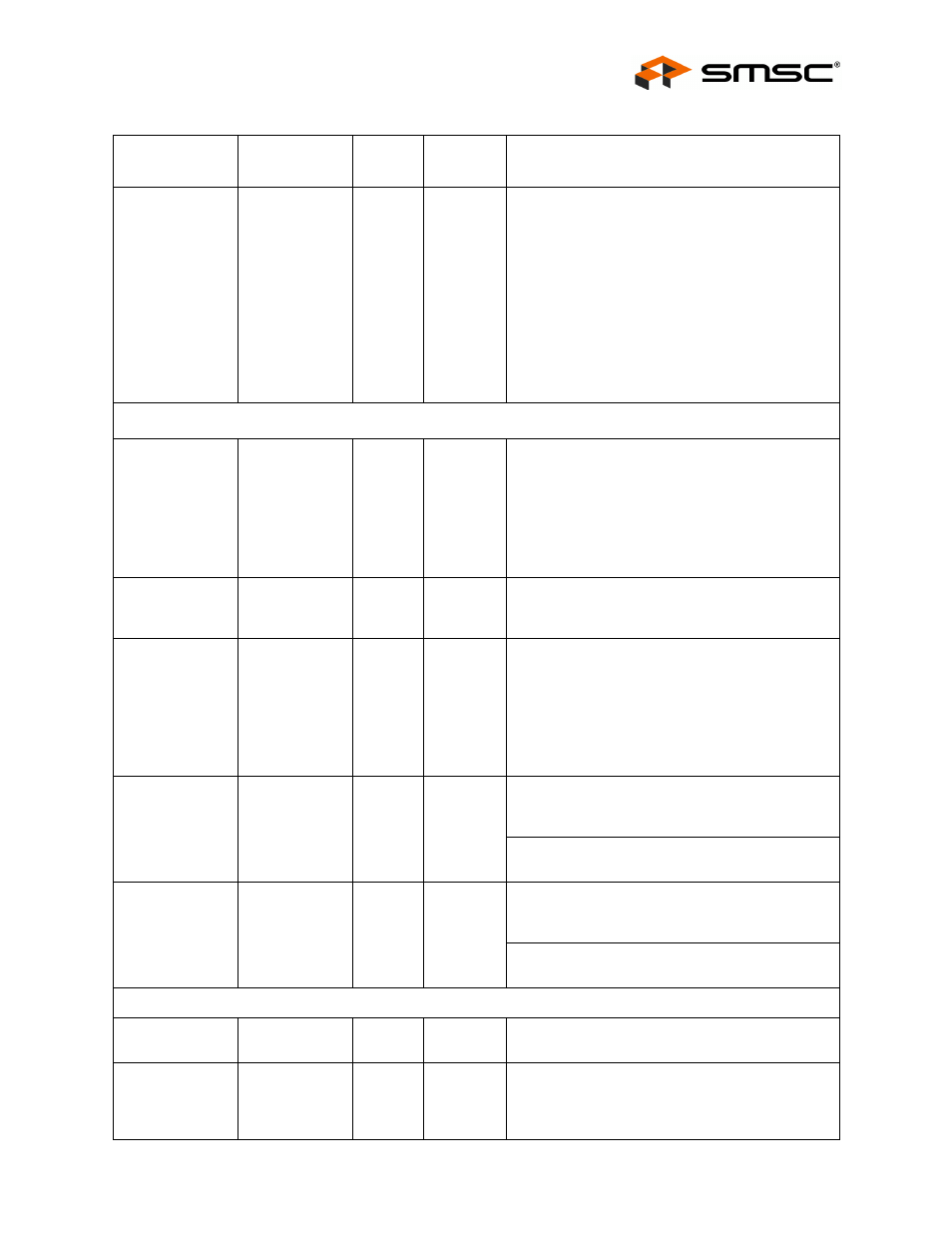
MS System Data
In/Out
MS_D[7:0]
20
19
17
18
32
30
23
24
I/O12PD
These pins are the bi-directional data signals for
the MS device. In serial mode, the most significant
bit (MSB) of each byte is transmitted first by either
MSC or MS device on MS_D0.
MS_D0, MS_D2, and MS_D3 have weak pull-
down resistors. MS_D1 has a pull down resistor if
in parallel mode, otherwise it is disabled. In 4 or 8
bit parallel modes, there is a weak pull-down
resistor on all MS_D7 - MS_D0 signals.
The resistors are controlled by MSC_SYSTE_0,
MSC_MODE_CTL and MSC_PRO_HG registers.
SECURE DIGITAL / MULTIMEDIACARD INTERFACE
SD Data 7-0
SD_D[7:0]
19
20
23
30
32
33
17
18
I/O12PU
These are the bi-directional data signals SD_D0-
SD_D7.
SD_D0 - SD_D7 have weak pull-up resistors.
SD Clock
SD_CLK
21
O12
This is an output clock signal to SD/MMC device.
The clock frequency is software configurable.
SD Command
SD_CMD
24
I/O12PU
This is a bi-directional signal that connects to the
CMD signal of the SD/MMC device.
The bi-directional signal should have an internal
weak pull-up resistor.
The pull-up register can be controlled by:
SD_MMC_INTF_EN bit of SDC_MODE CTL.
SD Write
Protected GPIO
GPIO6 /
SD_WP
13
I/O12
GPIO: This general purpose pin may be used
either as input, edge sensitive interrupt input, or
output.
SD_WP: This is a GPIO designated as the Secure
Digital card mechanical write detect pin.
SD Card Detect
GPIO
GPIO15 /
SD_nCD
14
I/O12
GPIO:This general purpose pin may be used
either as input, edge sensitive interrupt input, or
output.
SD_nCD: This is a GPIO designated as the
Secure Digital card detection pin.
USB INTERFACE
USB Bus Data
USB-
USB+
43
42
I/O-U
These pins connect to the upstream USB bus data
signals.
USB Bus Data
USBDN_DM
[3:2]
USBDN_DP
[3:2]
3
1
4
2
I/O-U
These pins connect to the downstream USB bus
data signals.
Table 6.1 USB2640/USB2641 Pin Descriptions (continued)
NAME
SYMBOL
48-PIN
QFN
BUFFER
TYPE
DESCRIPTION