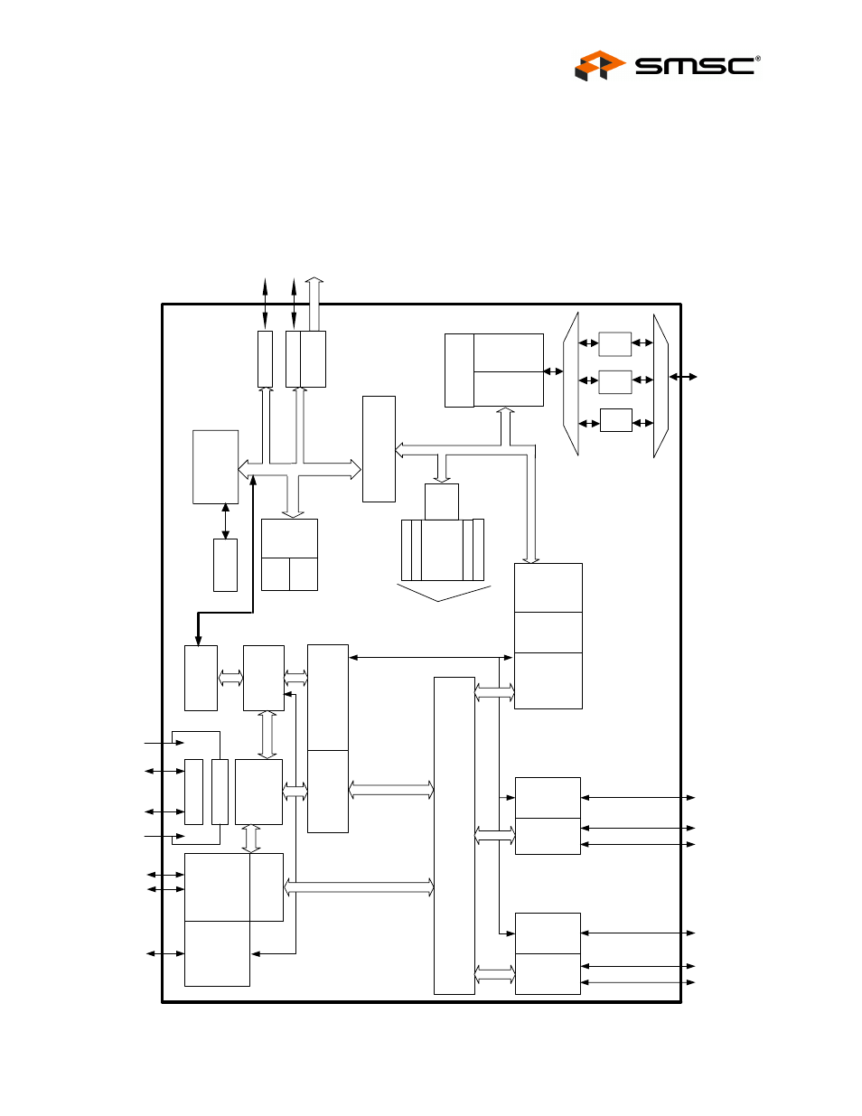
Chapter 5 block diagrams, Figure 5.1 usb2640 block diagram, Datasheet – SMSC USB2640i User Manual
Page 15
Ultra Fast USB 2.0 Multi-Format Flash Media Controller/USB Hub Combo
SMSC USB2640/USB2641
15
Revision 2.0 (10-03-08)
DATASHEET
Chapter 5 Block Diagrams
Figure 5.1 USB2640 Block Diagram
To
Upstr
eam
V
BU
S
3.
3V
Upst
re
am
PH
Y
Upst
rea
m
US
B
Dat
a
Repea
ter
Co
ntr
o
lle
r
Ser
ial
In
ter
face
Engin
e
Se
ri
al
Inte
rf
ace
PLL
24
MH
z
Cr
ys
ta
l
Ro
uting
& P
o
rt
Re
-Or
d
er
ing Log
ic
P
o
rt
C
o
n
tro
lle
r
PH
Y
Port
#
3
OC
Se
ns
e
Sw
it
ch
D
ri
ver
Bu
s
-P
o
w
er
D
e
tect
/V
BU
S
Pul
s
e
1.8
V
Tr
ansa
cti
o
n
Tr
ansl
ator
1.
8V Reg
PHY
Por
t #
2
OC
Se
ns
e
Sw
it
ch
Dr
iv
e
r
USB Data
Downstr
eam
OC
S
en
se
/
Pw
r Sw
itch
8051
PROCES
SOR
SF
R
RAM
XDATA
BRI
DGE
+ BU
S
ARBIT
E
R
RO
M
64K
RA
M
6K
ADDR
MAP
GPIOs
P
ro
g
ra
m
M
emo
ry
I
/O
B
u
s
PWR
_F
E
T0
6 p
ins
G
P
IO10 (
CRD
_PW
R
)
3K
to
ta
l
RA
M
EP2
TX
EP2
RX
BUS
INT
F
C
EP
0 T
X
EP0
RX
SI
E
CT
L
BRIDGE
BU
S
IN
TFC
FMDU
CT
L
AUTO_
CBW
PROC
FMI
BUS
INTF
C
USB Dat
a
Downs
tr
e
am
Fl
as
h Media
Cards
(r
e
q
uir
e Combo
soc
ket
)
MS
xD
SD
/
MMC
O
C
S
en
se/
Pw
r Swi
tc
h
SPI
SPI /
GPIO
(2
pin
s
)