Datasheet – SMSC USB2640i User Manual
Page 18
Ultra Fast USB 2.0 Multi-Format Flash Media Controller/USB Hub Combo
Revision 2.0 (10-03-08)
18
SMSC USB2640/USB2641
DATASHEET
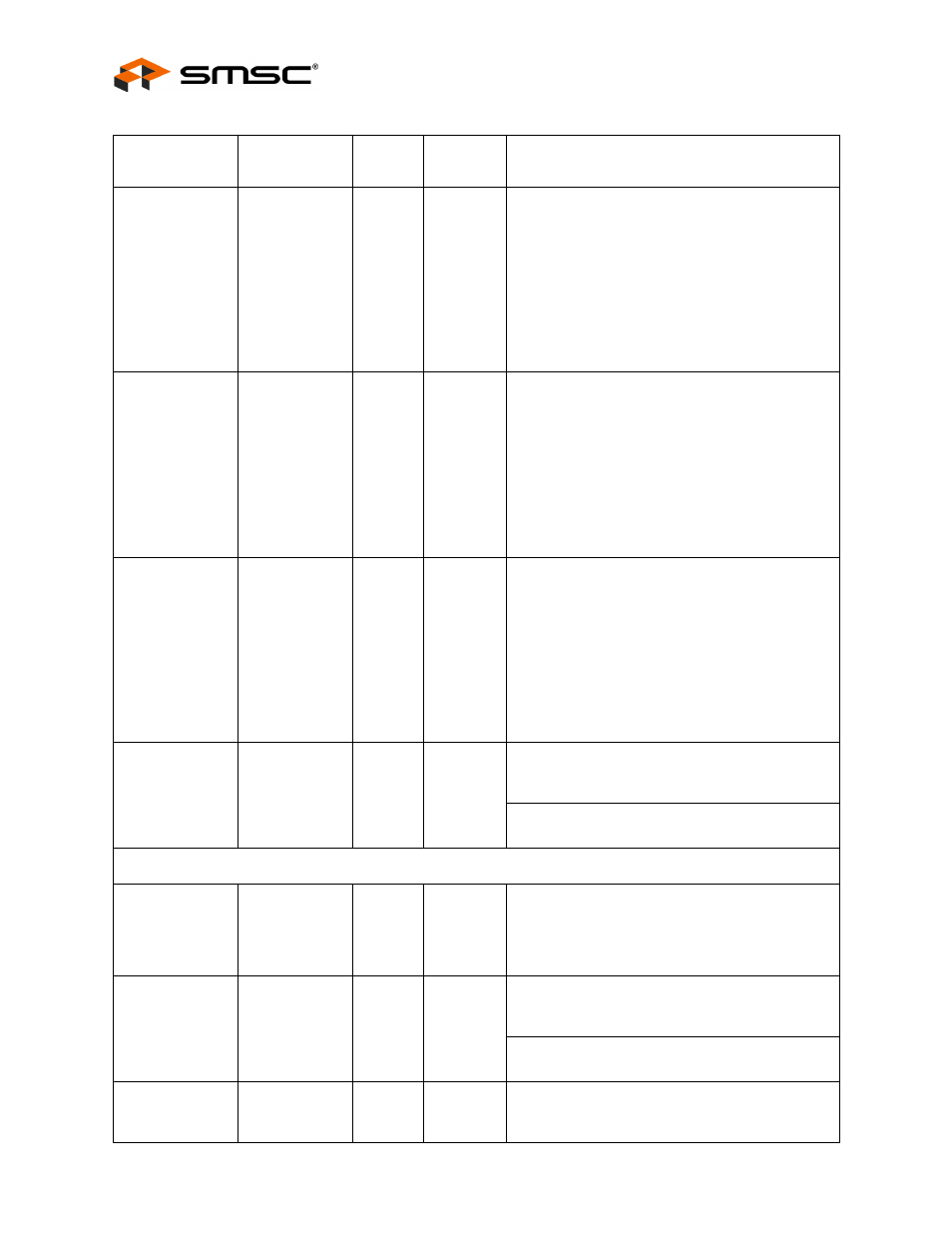
xD Write Enable
xD_nWE
22
O12PU
This pin is an active low write strobe signal for the
xD device.
When using the internal FET, this pin has an
internal weak pull-up resistor that is tied to the
output of the internal Power FET, and is controlled
by the xD_PU bit of the xDC_CTL register.
If an external FET is used (Internal FET is
disabled), then the internal pull-up is not available
(external pull-ups must be used).
xD Busy or Data
Ready
xD_nB/R
28
IPU
This pin is connected to the BSY/RDY pin of the
xD device.
When using the internal FET, this pin has an
internal weak pull-up resistor that is tied to the
output of the internal Power FET, and is controlled
by the xD_PU bit of the xDC_CTL register.
If an external FET is used (Internal FET is
disabled), then the internal pull-up is not available
(external pull-ups must be used).
xD Chip Enable
xD_nCE
26
O12PU
This pin is an active low chip enable signal for the
xD device.
When using the internal FET, this pin has an
internal weak pull-up resistor that is tied to the
output of the internal Power FET, and is controlled
by the xD_PU bit of the xDC_CTL register.
If an external FET is used (Internal FET is
disabled), then the internal pull-up is not available
(external pull-ups must be used).
xD Card
Detection GPIO
GPIO14 /
xD_nCD
29
I/O12
GPIO: This general purpose pin may be used
either as input, edge sensitive interrupt input, or
output.
xD_nCD: This is a GPIO designated as the xD-
Picture Card detection pin.
MEMORY STICK INTERFACE
MS Bus State
MS_BS
21
O12
This pin is connected to the BS pin of the MS
device.
It is used to control the Bus States 0, 1, 2, and 3
(BS0, BS1, and BS3) of the MS device.
MS Card
Insertion GPIO
GPIO12 /
MS_INS
31
IPU
GPIO: This general purpose pin may be used
either as input, edge sensitive interrupt input, or
output.
MS_INS: This is a GPIO designated as the
Memory Stick card detection Pin.
MS System CLK
MS_SCLK
13
O12
This pin is an output clock signal to the MS device.
The clock frequency is software configurable.
Table 6.1 USB2640/USB2641 Pin Descriptions (continued)
NAME
SYMBOL
48-PIN
QFN
BUFFER
TYPE
DESCRIPTION