0 signal description, Signal description – Intel D15343-003 User Manual
Page 27
Signal Description
D15343-003
27
3.0
Signal Description
This section describes the Intel
®
82854 GMCH signals. These signals are arranged in functional
groups according to their associated interface. The following notations are used to describe the
signal type.
The signal description also includes the type of buffer used for the particular signal:
Note:
System Address and Data Bus signals are logically inverted signals. In other words, the actual
values are inverted from what appears on the system bus. This must be taken into account and the
addresses and data bus signals must be inverted inside the GMCH. All processor control signals
follow normal convention: A 0 indicates an active level (low voltage), and a 1 indicates an active
level (high voltage).
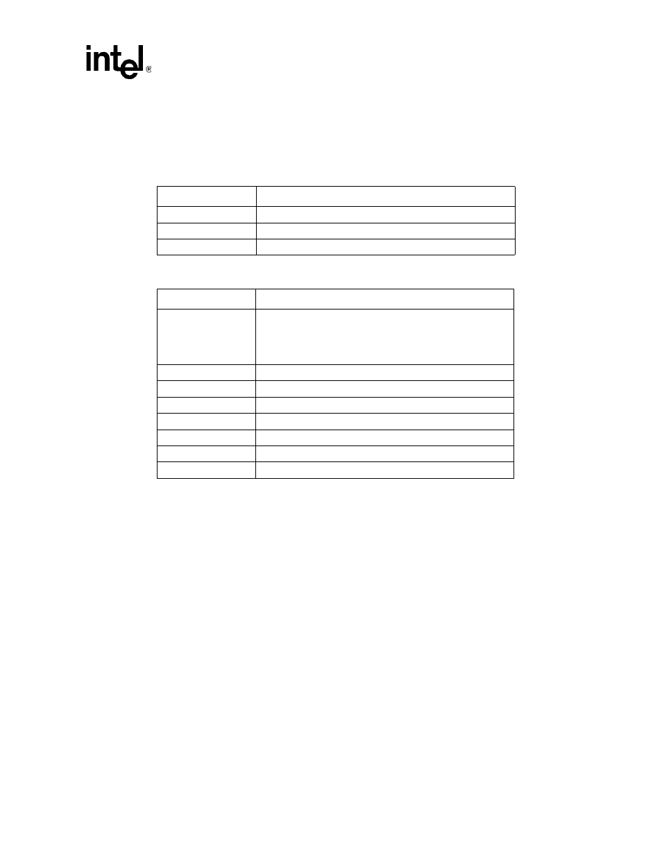
Notation
Description
I
Input pin
O
Output pin
I/O
Bi-directional Input/Output pin
Buffer
Description
AGTL+
Open Drain AGTL+ interface signal. Refer to the AGTL+ I/O
Specification for complete details. The GMCH integrates AGTL+
termination resistors, and supports VTTLF of 1.05 V ± 5%. AGTL+
signals are "inverted bus" style where a low voltage represents a
logical 1.
DVO
DVO buffers (1.5-V tolerant)
Hub
Compatible to Hub interface 1.5
SSTL_2
Stub Series Termination Logic compatible signals (2.5-V tolerant)
LVTTL
Low Voltage TTL compatible signals (3.3-V tolerant)
CMOS
CMOS buffers (3.3-V tolerant)
Analog
Analog signal interface
Ref
Voltage reference signal