Return path – Motorola BT100 User Manual
Page 22

Overview 2-11
BT100 Installation and Operation Manual
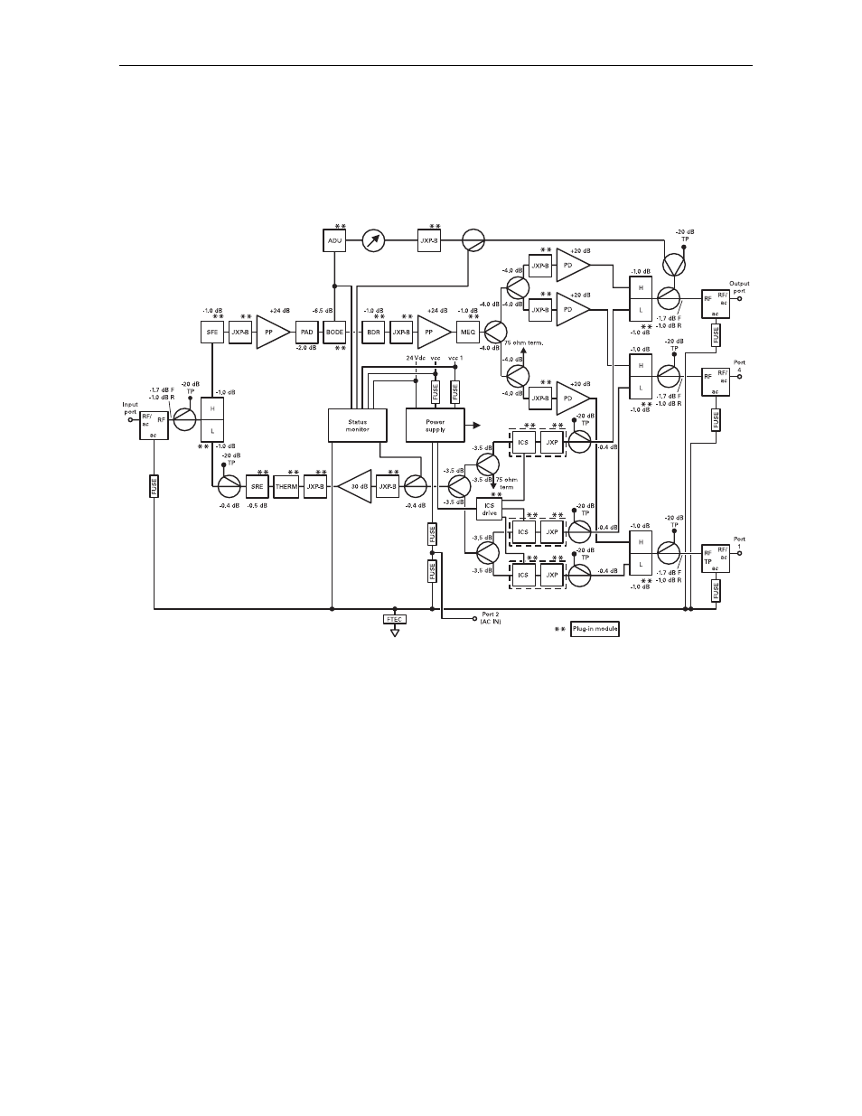
Figure 2-11 illustrates the interconnection between these components in the three output
BT100*-3*.
Figure 2-11
BT100*-3* three output block diagram
Return Path
The BT100 main amplifier circuit board includes the return path. This equips the BT100 to pass
signals in the return or upstream direction. The standard circuit board contains all components
including the diplex filters with extended return bandwidth for the amplifier input and output.
Optional SRE-*-* return equalizers compensate for cable attenuation and are available in 1 dB
increments for S-split, and 2 dB increments for all other splits, from 0 dB through 12 dB. You
must install a return equalizer to activate the return path.
There are JXP-*B pad facilities located at the inputs and output of the return path. You can use
these pad facilities as test points or signal injection points. The output pad value is normally
selected to control the return signal level into the next upstream amplifier, while the input pad
value is selected to attenuate excessive input signal.
The return-input test points and the return-output test point are –20 dB directional couplers.
These test points present a 75-ohm source impedance and do not require special test probes.
Optional return path thermal compensation is provided by plug-in JXP-TH2C or JXP-TH3C
modules that stabilize gain and match over temperature extremes.
