Avago Technologies ACPL-336J-000E User Manual
Page 4
4
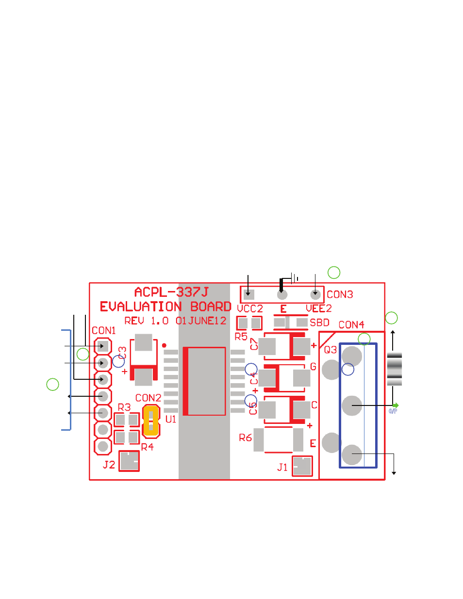
Gnd
Vin+
Vcc1
/Fault
LED+
LED
-
/UVLO
+5
V
Gn
d
DC
Su
pp
ly
1
+1
5 V
–5
V
0 V
DC Supply 2
DC Supply 3
2
3
4
5a
5c
5d
IGBT
HV+
HV–
Gnd
IN+
Microcontroller
O/P
1
5b
6
Inductive Load
Practical Connections of the Evaluation board Using Power MOSFET for Actual Inverter Test
1. Solder an actual IGBT at Q3 by following the pins marked as G (gate), C (collector) and E (emitter).
2. Connect a +5V DC supply (DC supply 1) across V
CC1
and GND terminals of CON1.
3. Connect another DC supply (DC Supply 2 of +15V) across V
CC2
(V
CC2
pin) and V
E
(E pin) terminals of CON3. Connect
a third DC supply (DC Supply 3 of -5V typical or -15V max) across V
EE2
(V
EE2
pin) and V
E
(E pin) terminals of CON3.
Maximum voltage across V
CC2
and V
EE2
is 30 V. These two DC power supplies must be isolated from DC Supply 1.
4. Connect the PWM output signals(meant to drive the IGBT) from microcontroller to input signals at IN+ and Gnd pins
of CON1; Connect also the /UVLO and /Fault from CON1 to the same microcontroller at designated feedback pins.
5. Use a multi-channel Digital Oscilloscope to capture the waveforms at the following points:
a. Input PWM signal at IN+ pin (CON1) with reference to (w.r.t.) Gnd
b. V
G
representing the gate drive voltage of ACPL-337J (U1) at G (gate) pin of Q3 w.r.t. E (emitter) pin. Monitoring of
this signal must be done through a HV differential probe
c. Desat signal at pin 14 of U1 represents the Desat voltage of IGBT’s C (collector) pin during turn-on. Monitoring of
this signal must be done through a HV differential probe
d. Miller Clamp voltage of IGBT at pin 10 of U1. Monitoring of this signal must be done through a HV differential
probe
6. Connect C (collector) pin of the IGBT to HV+ (High Voltage DC Bus+) through a properly selected Inductive Load.
Connect E (emitter) pin of the IGBT to HV- (High Voltage DC Bus-). (Note: It is advised to enable the current limiting
function of the HV Power Source supplying the High Voltage DC Bus voltage during this test to protect the Inverter
and its drive circuits). Maximum voltage allowed across HV+ and HV- is 1 kV for the board.
Figure 4. Connection of evaluation board in actual applications