Testing igbt gate driver (in simulation mode) – Avago Technologies ACPL-336J-000E User Manual
Page 2

2
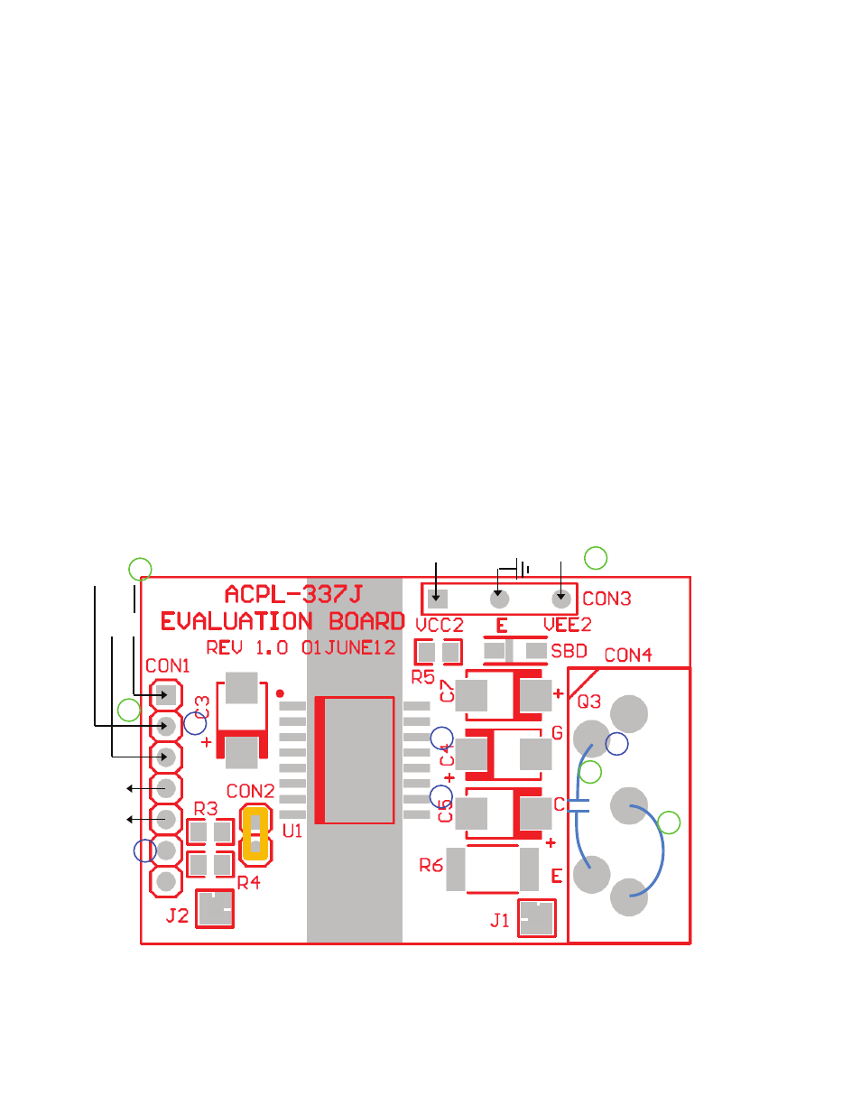
Testing IGBT Gate Driver (in Simulation Mode)
1. Solder a 10 nF capacitor across the Gate and Emitter terminals of Q3 (to simulate actual gate capacitance of an IGBT).
2. Solder a jumper wire across the Collector and Emitter terminals of Q3 (to simulate a turn-on saturated Collector
voltage of IGBT).
3. Connect a +5V DC supply (DC supply 1) across V
CC1
and GND terminals of CON1.
4. Connect another DC supply (DC Supply 2 of +15 V typical or +30 V maximum) across V
CC2
(V
CC2
pin) and V
E
(E pin)
terminals of CON3. Connect a third DC supply (DC Supply 3 of -5V typical or -15 V maximum) across V
EE2
(V
EE2
pin)
and V
E
(E pin) terminals of CON3. Maximum voltage across V
CC2
and V
EE2
is 30 V. For testing, these power supplies
can be non-isolated.
5. Connect a 10 kHz 5 V DC pulse (at about 50% duty) from a dual-output signal generator across IN+ and Gnd pins of
CON1 to simulate microcontroller output to drive the IGBT.
6. Use a multichannel digital oscilloscope to capture the waveforms at the following points:
a. Input PWM signal at IN+ pin (CON1) with reference to (w.r.t.) Gnd.
b. LED signal at LED+ pin w.r.t. Gnd (or LED-). Note: this is a generated LED drive signal from the device ACPL-337J.
c. V
G
representing the gate drive voltage of ACPL-337J (U1) at G (gate) pin of Q3 w.r.t. E (emitter) pin.
d. Desat signal at pin 14 of U1, which represents the Desat voltage of IGBT’s C (collector) pin during turn-on.
e. Confirm that LED+ signal is almost identical to IN+ signal, and then switch this channel to monitor the simulated
Miller Clamp voltage of IGBT at pin 10 of U1.
7. Provision is done on the board to allow for the LED to be driven directly by 5 V PWM (10 kHz) signals instead of the IN+
signal by disconnecting the shunt post at CON2. Once the shunt post at CON2 is removed, the external PWM signals
(at 10 kHz 5V
PP
) can be connected directly to LED+ and LED- pins at CON1.
Note:
Before you proceed to the next tests, make sure you remove the jumper wire that was connected in Step 2.
Figure 2. Simple Simulation Test Setup of Evaluation board
Gnd
Vin+
Vcc1
/Fault
LED+
LED-
/UVLO
+5
V
Gn
d
DC
Su
pp
ly
1
Si
gn
al
In
pu
t
in
+
+1
5V
–5
V
0V
DC Supply 2
DC Supply 3
10 nF
Jumper
Short
1
2
3
4
5
6a
6b
6c
6d
6e
