Chapter 3, Board layout – Lanner LVC-5570 User Manual
Page 25
25
Board Layout
Chapter 3
Embedded and Industrial Computing
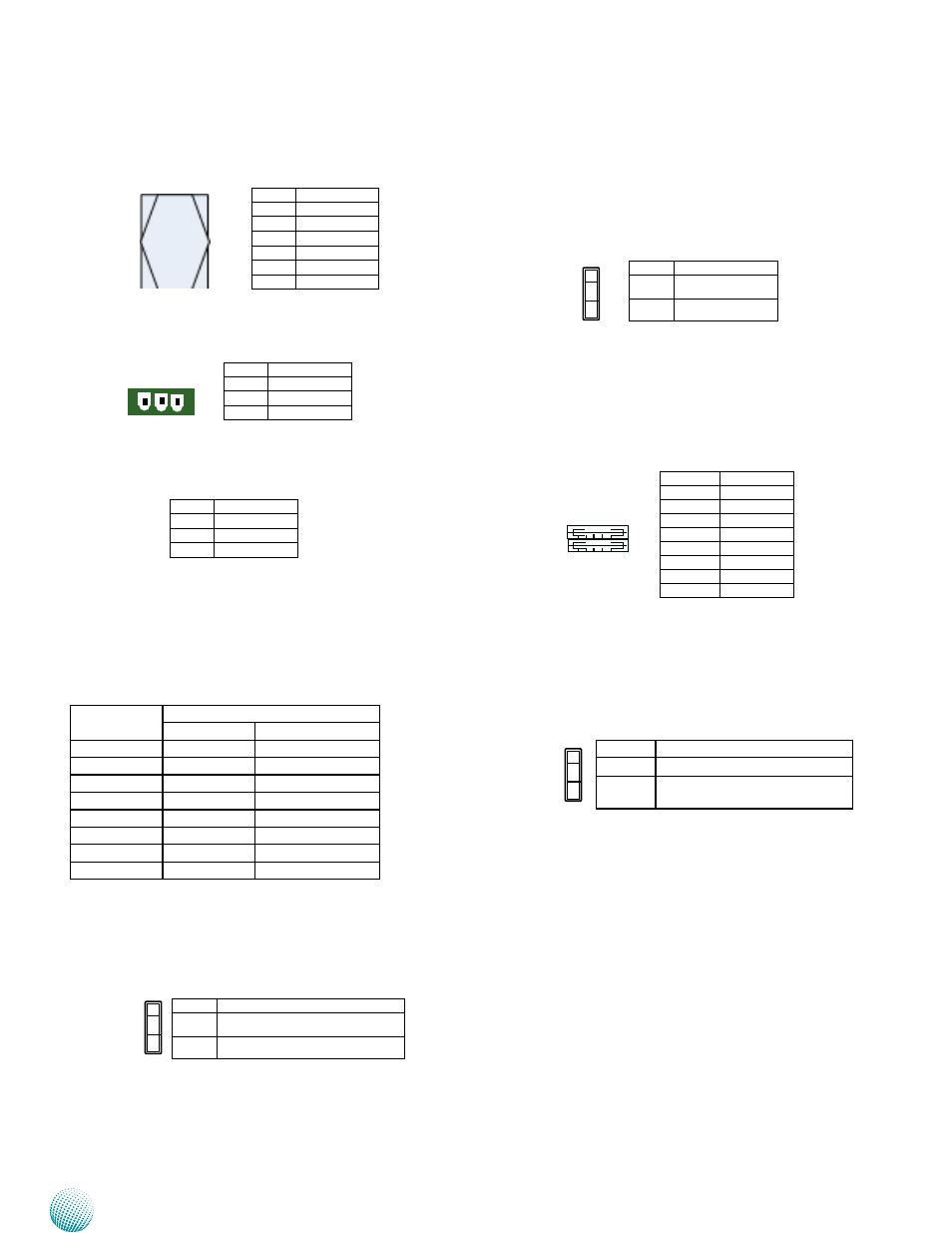
SIM Card Socket (SIM1):
CN3: A power connector with power -ignition Control
DCJK1 (Optional): An optional DC Jack type of Power
Connector
LAN1/LAN2 Ports (LAN1/LAN2): The LAN ports are
provided by Intel 82574L Ethernet controller whose
interface complies with PCI-e 1.1 (2.5 Ghz). It has advanced
management features including IPMI pass-through via
SMBus or NC-SI, WOL, PXE remote boot, ISCSI boot and
VLAN filtering.
Pin No.
Description
Fast Ethernet Gigabit Ethernet
1
TX+
BI_DA+
2
TX-
BI_DA-
3
RX+
BI_DB+
4
--
BI_DC+
5
--
BI_DC-
6
RX-
BI_DB-
7
--
BI_DD+
8
--
BI_DD-
Enable or Disable Daughter Board LEK-IOA6 (COMSLT1):
This jumper is for enabling or disabling COM3/COM4 of
daughter board LEK-IOA6.
Pin No.
Pin Name
1
Ignition
2
GND
3
DC_VIN
Pin No.
Pin Name
1
DC_VIN
2
GND
3
GND
1 2 3
Enable or Disable Daughter Board LEK-IG1 (COMSLT2):
This jumper is for enabling or disabling COM5/COM6 of
daughter board LEK-IG1. If this jumper is set to disable,
the ISM will not work (refer to
Appendix A Using the Ignition
System Manager (ISM)).
Dual USB 2.0 Port Connector #0 and #1 (USB1)
Dual USB 2.0 Port Connector #2 and #3 (USB2)
Dual USB 2.0 Port Connector #4 and #5 (USB3)
Clear CMOS jumper (CMOS1/CMOS2): It is for clearing
the CMOS data. CMOS 1clears CMOS data with real-time
clock (RTC) whereas CMOS2 clears CMOS data only.
To erase the CMOS data:
Turn off the computer and unplug the power cord.
Move the jumper cap from pins 1-2 (default) to pins
1.
2-3. Keep the cap on pins 2-3 for about 5-10 seconds,
then move the cap back to pins 1-2.
Plug the power cord and turn on the computer.
2.
Enter BIOS setup to re-enter data.
3.
Pin No.
Pin Name
1-2
Disable
2-3
Enable
Pin No.
Pin Name
1-2
Disable
2-3
Enable
1
2
3
1
2
3
1 2 3 4
5 6 7 8
Pin No.
Pin Name
1
VCCUSB
2
USB0N
3
USB0P
4
GND
5
VCCUSB1
6
USB1N
7
USB1P
8
GND
Pin No.
Pin Name
1-2
Normal (Default)
2-3
Clear CMOS and RTC (CMOS1)
Clear CMOS only (CMOS2)
1
2
3
Pin No.
Description
C1
UIM_PWR
C2
UIM_RST
C3
UIM_CLK
C5
GND
C6
UIM_VPP
C7
UIM_DAT
C5 C7
C1 C3