Chapter 3, Board layout – Lanner LVC-5570 User Manual
Page 21
21
Board Layout
Chapter 3
Embedded and Industrial Computing
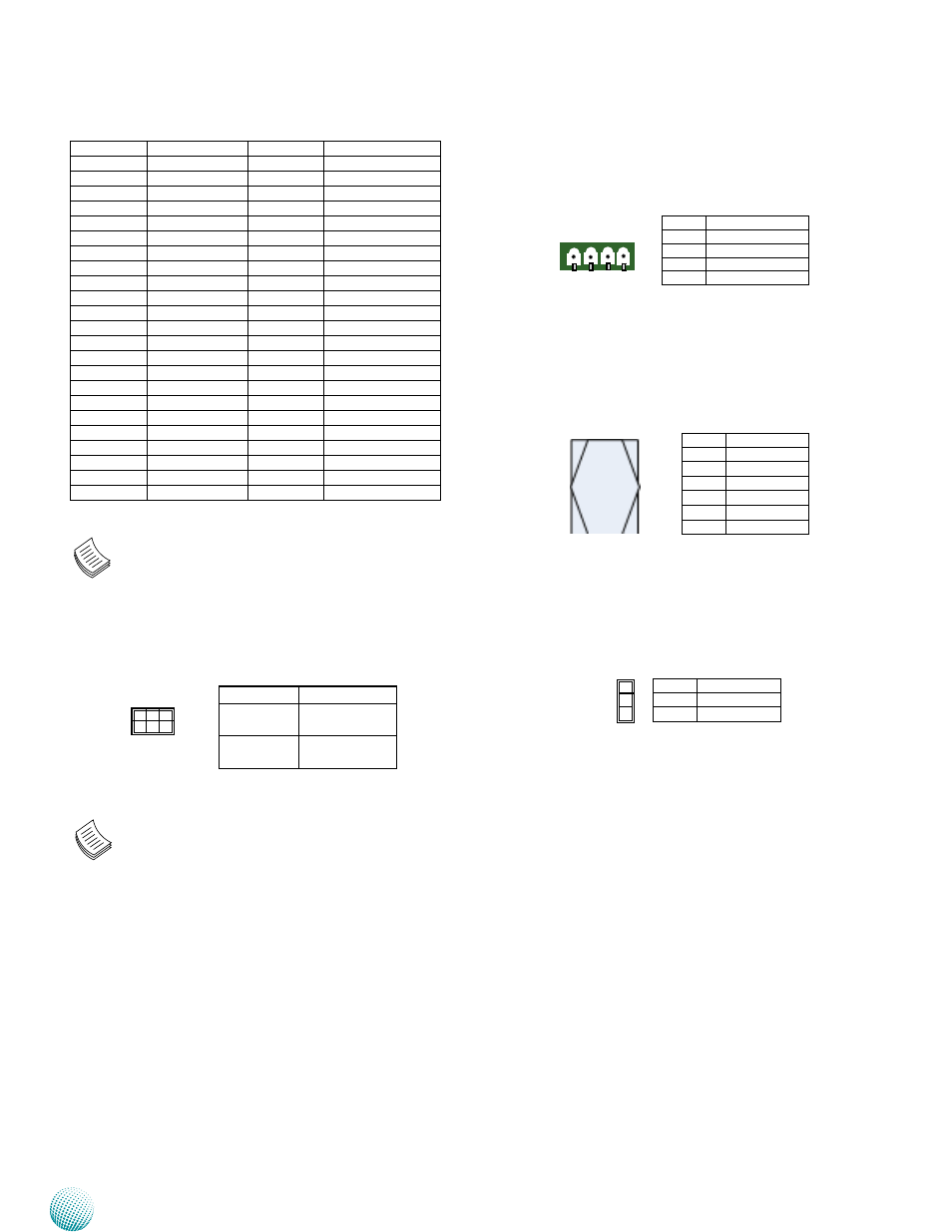
DC Relay Bypass (CN2) : 9~30V, 10A DC power input and
output Integrated in a 4-pin terminal.
SIM Card Socket (SIM1/SIM2): SIM1 and SIM2 are paired
with connector MPCIE1 and MCARD1 respectively.
Select MCARD1 Voltage for Module Sierra MC809x
(J6) : The default is 3.3V for most 3G mini card; for Sierra
Airprime HSPA+ mini card , set it to +3.6V.
4 3 2 1
Pin No.
Function
1
P930V
2
GND
3
GND_930V
4
P930V_OUT
Pin No.
Description
C1
VREG
C2
USIM_RESET
C3
USIM_CLK
C5
GND
C6
USIM_VPP
C7
USIM_DATA
C5 C7
C1 C3
Pin
Signal
Pin
Signal
7
N/A
8
VREG_USIM2
9
GND
10
UIM2_DATA
11
N/A
12
UIM2_CLK
13
N/A
14
UIM2_RESET
15
GND
16
UIM2_VPP
17
N/A
18
GND
19
N/A
20
RF_KILL_2
21
GND
22
N/A
23
N/A
24
VCC3P6_MINI1
25
N/A
26
GND
27
GND
28
N/A
29
GND
30
N/A
31
N/A
32
3G_WAKE_MCU
33
3G_RESET_N
34
GND
35
GND
36
PCH_USB_N12
37
GND
38
PCH_USB_P12
39
VCC3P6_MINI1
40
GND
41
VCC3P6_MINI1
42
3G_LED2_WWAN_N
43
GND
44
N/A
45
PCM_CLK
46
N/A
47
PCM_DIN
48
N/A
49
PCM_OUT
50
GND
51
PCM_SYNC
52
VCC3P6_MINI1
Note: Jumper J6 is used to select power voltage
for MCARD1.
Enable or disable the onboard SSD memory (HDDSL1)
Note: When trying to install an OS on the external
SATA 2.5 hard disk or SSD, disable it first by setting
the jumpers accordingly. Enable it after finishing
the OS installation.
Pin No.
Description
1-2
3.3V
2-3
3.6V
1
2
3
Pin No.
Pin Name
1-3 short
2-4 short
Enable (default)
3-5 short
4-6 short
Disable
5
6
1
2