Chapter 3, Board layout – Lanner LVC-2000 User Manual
Page 18
18
Board Layout
Chapter 3
Embedded and Industrial Computing
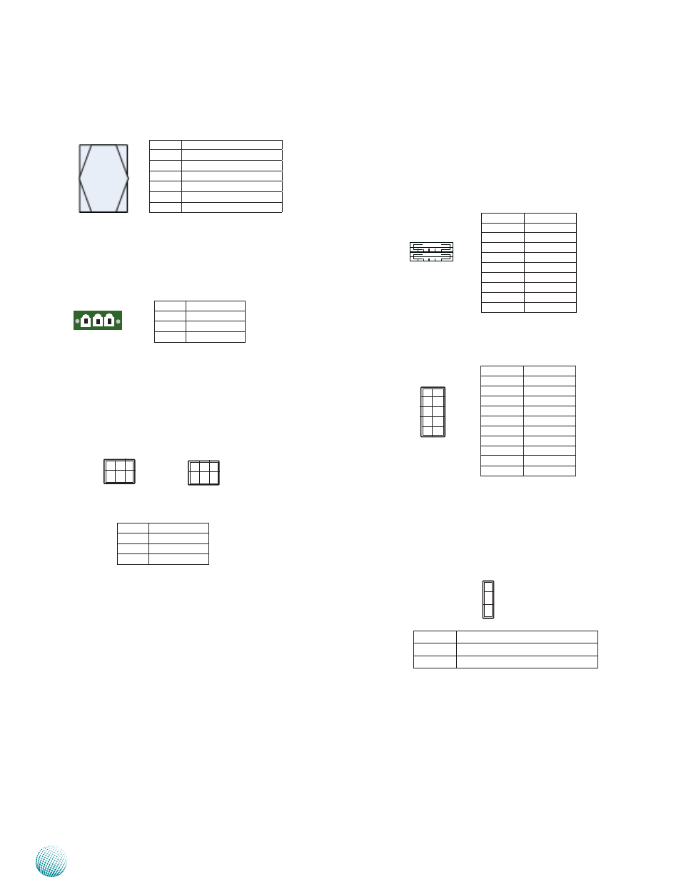
SIM Card Socket (SIM1): SIM1 pairs with MPCIE1 and
SIM2 pairs with MPCIE2.
Power-in with Ignition Control (PRJK1): A power
connector with power -ignition Control
COM1/COM2 Power Selection (JRI1/JRI2): JRI1 selects
COM1 power voltage and JRI2 selects COM2 power voltage
. The default is Ring Indicator (RI) for pin 8.
USB 2.0 Pin Header for USB 0, USB1 (USBF1)
USB 3.0 Port Connector for USB2 (USB2)
Clear CMOS (JCMOS1):
Pin No.
Pin Name
1
Ignition
2
GND
3
DC_VIN
3 2 1
1 2 3 4
5 6 7 8
Pin No.
Pin Name
1
VCCUSB2
2
USB0N2
3
USB0P2
4
GND
5
USB3_SSRXN
6
USB3_SSRXP
7
GND
8
USB_SSTXP
9
USB_SSTXN
Pin No.
Pin Name
1-2
Normal (Default)
2-3
Clear RTC
Pin No.
Description
C1
UIM_PWR
C2
UIM_RST
C3
UIM_CLK
C5
GND
C6
UIM_VPP
C7
UIM_DAT
C5 C7
C1 C3
Pin No.
Pin Name
1
VCC5
2
GND
3
N/A
4
USBDDP1
5
USBDN0
6
USBDN1
7
USBDP0
8
N/A
9
GND
10
VCC5
1
3
5
7
9
2
4
6
8
10
2
1
6
5
JRI1
2
1
6
5
JRI2
Pin No.
Signal
1-2
Default
3-4
VCC5
5-6
VCC12
- LVC-5000(N4) (42 pages)
- LVC-5550S (41 pages)
- LVC-5570 (48 pages)
- LVC-5770 (49 pages)
- FW-6432 (16 pages)
- FW-7525 (41 pages)
- FW-5330 (38 pages)
- FW-6486 (18 pages)
- FW-6436 (19 pages)
- FW-7573 (44 pages)
- FW-7568 (52 pages)
- FW-7540 (47 pages)
- FW-8759 (47 pages)
- FW-7581 (23 pages)
- FW-8758 (42 pages)
- FW-7610 (44 pages)
- FW-8756 (24 pages)
- FW-7575 (48 pages)
- FW-8760 (53 pages)
- FW-8877 (46 pages)
- FW-8892 (58 pages)
- FW-8893C (49 pages)
- FX-3411 (48 pages)
- FW-8894 (31 pages)
- FW-8771 (47 pages)
- RS12-38800 (64 pages)
- MR-320 (20 pages)
- FX-3210 (54 pages)
- MR-301 (16 pages)
- MR-350 (12 pages)
- MR-330A (16 pages)
- MR-730 (18 pages)
- VES-220 (19 pages)
- VES-270 (19 pages)
- VES-310 (15 pages)
- VES-310 V2 (20 pages)
- VES-500 (21 pages)
- EM-F345 (30 pages)
- VES-8X2 (16 pages)
- VES-8X6 (17 pages)
- LEC-2026 (67 pages)
- LEC-2010 (65 pages)
- LEC-2136 (20 pages)
- LEC-2050 (38 pages)