Chapter 3, Board layout, Jumper settings – Lanner LVC-2000 User Manual
Page 15
15
Board Layout
Chapter 3
Embedded and Industrial Computing
Maximum input/output current for each port is
100mA
For all Input/
output pins:
Voltage
Logic
Register
DI: <0.8V
DO: <0.4V
Low
0
DI:
10 ~ 12V
DO:12V
High
1
The default BIOS value is 0 for DI and 1 for DO
1. Pin3 and pin4 can be used for DI wake-up function
(Refer to the flow chart in Chapter 4 and the ISM in
Appendix A).
2. Pin 15, 16, 17 can be used for Digital output control
with contact current 9~36V@2A (DO1); Pin 18, 19,
20 can be used for digital output control with
contact current 9~36V@2A in maximum (DO2).
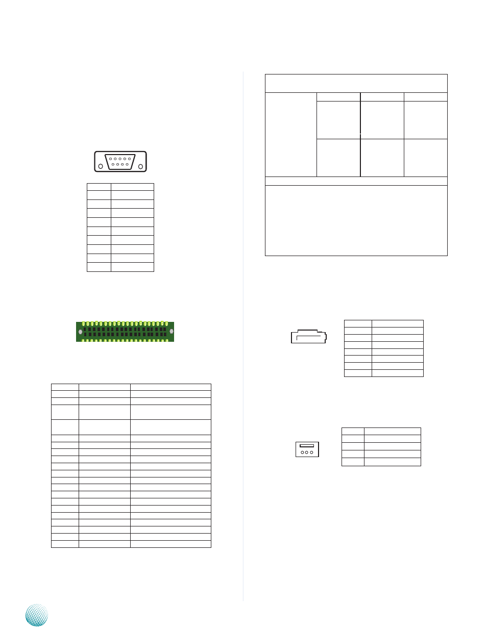
Serial-ATA Connector (SATA1): It is for connecting a 2.5’’
hard disk to be served as your system’s storage. It can
supports SATA 2.0.
4-pin Serial-ATA Power Connector (SATAPWR1): It is for
connecting the SATA power cord.
Jumper Settings
COM1 RS-232 Serial Port (COM1/COM2): An RS-232
port through the D-SUB9 connector. The RI (pin 8) can be
altered with jumper JRI1 and JRI2.
Multiple I/O Connectors (MIO1): Multiple I/O pins for
functions in serial communication, Digital In/Out, Ignition
detection input for automatic wake-up function
6 7 8 9
1 2 3 4 5
Pin No.
Pin Name
1
DCD
2
DSR
3
RXD
4
RTS
5
TXD
6
CTS
7
DTR
8
RI1
9
GND
25 1
26 2
Pin No.
Function
1
GND
2
SATATXP
3
SATATXN
4
GND
5
SATARXN
6
SATARXP
7
GND
Pin No.
Pin Name
1
VCC12
2
GND
3
GND
VCC5
SATAPWR1
1 2 3 4
SATA1
7 6 5 4 3 2 1
Pin No.
Function
Function
1
GND
2
12V_OUT
12VDC Power Output
3
IGN_DI0
Input pin for automatic
wakeup
4
IGN_DI1
Input pin for automatic
wakeup
5
EXT_TXD_R
COM_TxD
6
EXT_RXD_R
COM_RxD
7
DI_0
Digital-In_0
8
DO_0
Digital-Out_0
9
DI_1
Digital-In_1
10
DO_1
Digital-Out_1
11
DI_2
Digital-In 2
12
DO_2
Digital-Out 2
13
DI_3
Digital-In 3
14
DO_3
Digital-Out 3
15
RELAY1_NOPEN
RELAY1 Normally Open
16
RELAY1_COMM
RELAY1 Common
17
GND
Ground
18
GND
Ground
19
RELAY2_NOPEN
RELAY2 Normally Open
20
RELAY2_COMM
RELAY2 Common