Functional description, Input processing, Reclocking processing – Grass Valley 8949MDA-CFR v.1.0.X User Manual
Page 31: Hd to sd downscaling
8949MDA-CFR and 8949MDA-SFR Instruction Manual
31
Functional Description
Functional Description
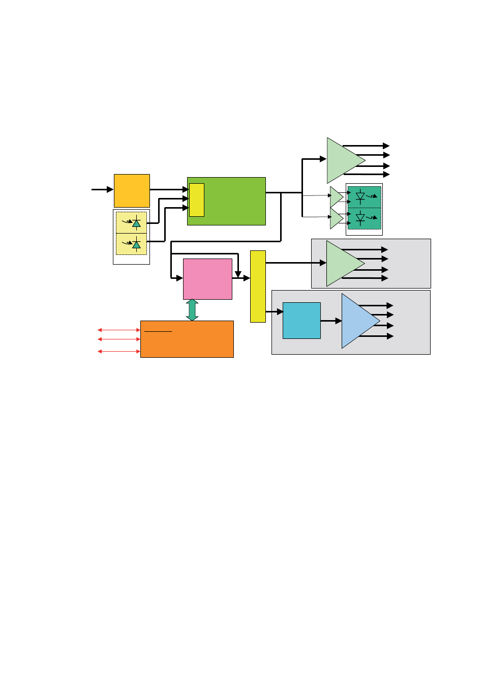
A block diagram of the 8949MDA is shown in
.
Figure 15. 8949MDA Block Diagram
Input Processing
The wideband serial SD or HD signal enters the module from rear BNC J9 to an
input amplifier. It is then equalized for the specified cable lengths in the equalizer
circuit and it is then reclocked.
Reclocking Processing
The signal then enters the reclocker circuit which reduces the jitter of the incoming
signal so as to ensure correct backward processing behavior.
HD to SD Downscaling
The incoming signal is in HD format. This block converts the signal to SD format
for monitoring applications.
Input
Equalizer
Core CPU
Control & Command process
_ Configuration
_ Alarming
Reclocker
Module
(Auto format
Detection)
Serial
SD/HD
input
Manual C&C
S
E
L
E
C
T
O
R
Frame bus
S
E
L
Board C&C
Serial
SD/HD
Outputs
SDI
Driver
Module
Serial
SD
Outputs
LEDs
HD to SD
Downscaler
Module
Encoder
NTSC/PAL
(10 bits quality)
8949MDA-CFR
8949MDA-SFR
Bypass if SD only
Composite
Video
Signal
Outputs
SD/HD
1310 nm
Single Mode
Optical inputs
Optional
SD/HD
1310 nm
Single Mode
Optical outputs
Optional
SDI
Driver
Module
Analog
Amplifier
Module
8434-07