Architecture description, Smt351 block diagram, Figure 1: smt351 board block diagram – Sundance SMT351 User Manual
Page 8: Xilinx fpga
Version 1.6
Page 8 of 25
SMT351 User Manual
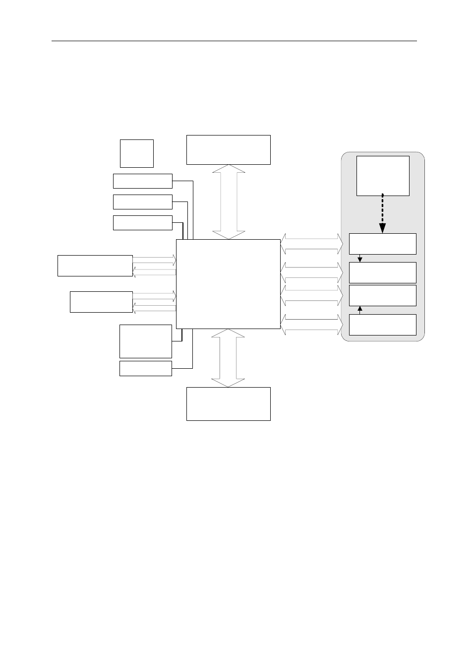
Architecture description
SMT351 block diagram
Figure 1 shows a block diagram of the SMT351 board. Refer to the following section
for additional information on the major blocks.
2 x RSL Connectors
(8 RSL Interfaces)
Xilinx FPGA
VirtexII-Pro, FF896
XC2VP7,20,30
1.5V Core
2.5/3.3V I/O
6-pin JTAG
header
J2 Bottom Secondary TIM
Connector
4x ComPorts/SDLs
J1 Top Primary TIM
Connector
2x ComPorts/SDLs
FPGA
configuration via
one of six
comports
40 I/O pins (D+@)
Clock + Feedback
2 x Sundance High-speed
Bus Connectors
40 I/O pins (D+@)
Clock + Feedback
128 (256) Mbytes DDR
RAM - MT46V16M16
40 I/O pins (D+@)
Clock + Feedback
128 (256) Mbytes DDR
RAM - MT46V16M16
40 I/O pins (D+@)
Clock + Feedback
4 LEDs + 4 TTL IOs
On-board Oscillator
50 MHz
External 5-Volt
Power Supply
converted to
2.5 Volts by a
DC-DC converter
128 (256) Mbytes DDR
RAM - MT46V16M16
128 (256) Mbytes DDR
RAM - MT46V16M16
3 Power
Supply
LEDs
‘FPGA configured’
LED
Figure 1: SMT351 board block diagram