Clock structure, Figure 5: fpga’s clock domains, Table 4: fpga’s clock domains description – Sundance SMT351 User Manual
Page 17
Version 1.6
Page 17 of 25
SMT351 User Manual
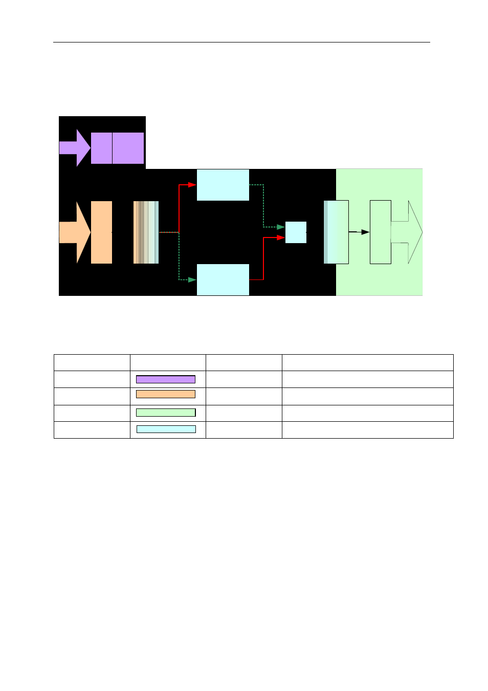
Clock structure
This section describes the various clock domains in the FPGA.
The figure below shows the four clock domains of the SMT351 design and their
interrelation.
SHB
A
SHB
B
Memory
compartment 0
Memory
compartment 1
Mux
400
MBytes/
sec
400
MBytes/
sec
Registers
Com
Port
Control
words
Input
buffer
Output
buffer
Input clock
domain
DDR SDRAM
clock domain
Output clock
domain
Figure 5: FPGA’s clock domains
Table 4: FPGA’s clock domains description
Clock domain
Colour
Frequency
Description
ComPort
50 MHz
Comport and registers clock
Data input
≤ 100 MHz
SHB A clock.
Data output
100 MHz
SHB B clock.
DDR SDRAM
100 MHz
DDR SDRAM clock.
See also other documents in the category Sundance Equipment:
- SMT107 (16 pages)
- SMT6035 v.2.2 (39 pages)
- SMT6012 v.4.6 (22 pages)
- FC100 (12 pages)
- FC108 v.1.1 (10 pages)
- SMT6065 v.4.0 (45 pages)
- FFT v.2.1 (19 pages)
- SMT111 (18 pages)
- SMT118LT (10 pages)
- SMT118 (20 pages)
- SMT123-SHB (13 pages)
- SMT128 (15 pages)
- SMT145 (18 pages)
- SMT148 (35 pages)
- SMT130 v.1.0 (46 pages)
- SMT148FX (48 pages)
- SMT310Q (55 pages)
- PARS (70 pages)
- SMT166-FMC (52 pages)
- SMT166 (44 pages)
- SMT300Q v.1.6 (61 pages)
- SMT310 v.1.6 (50 pages)
- SMT317 (24 pages)
- SMT326v2 (24 pages)
- SMT338 (19 pages)
- SMT349 (32 pages)
- SMT339 v.1.3 (27 pages)
- SMT338-VP (22 pages)
- SMT358 (25 pages)
- SMT351T (37 pages)
- SMT350 (45 pages)
- SMT362 (30 pages)
- SMT365G (23 pages)
- SMT364 (37 pages)
- SMT373 (15 pages)
- SMT368 (24 pages)
- SMT370v3 (46 pages)
- SMT377 (22 pages)
- SMT381 2007 (31 pages)
- SMT381-VP (81 pages)
- SMT387 (42 pages)
- SMT391 (18 pages)
- SMT384 (47 pages)
- SMT390-VP (55 pages)