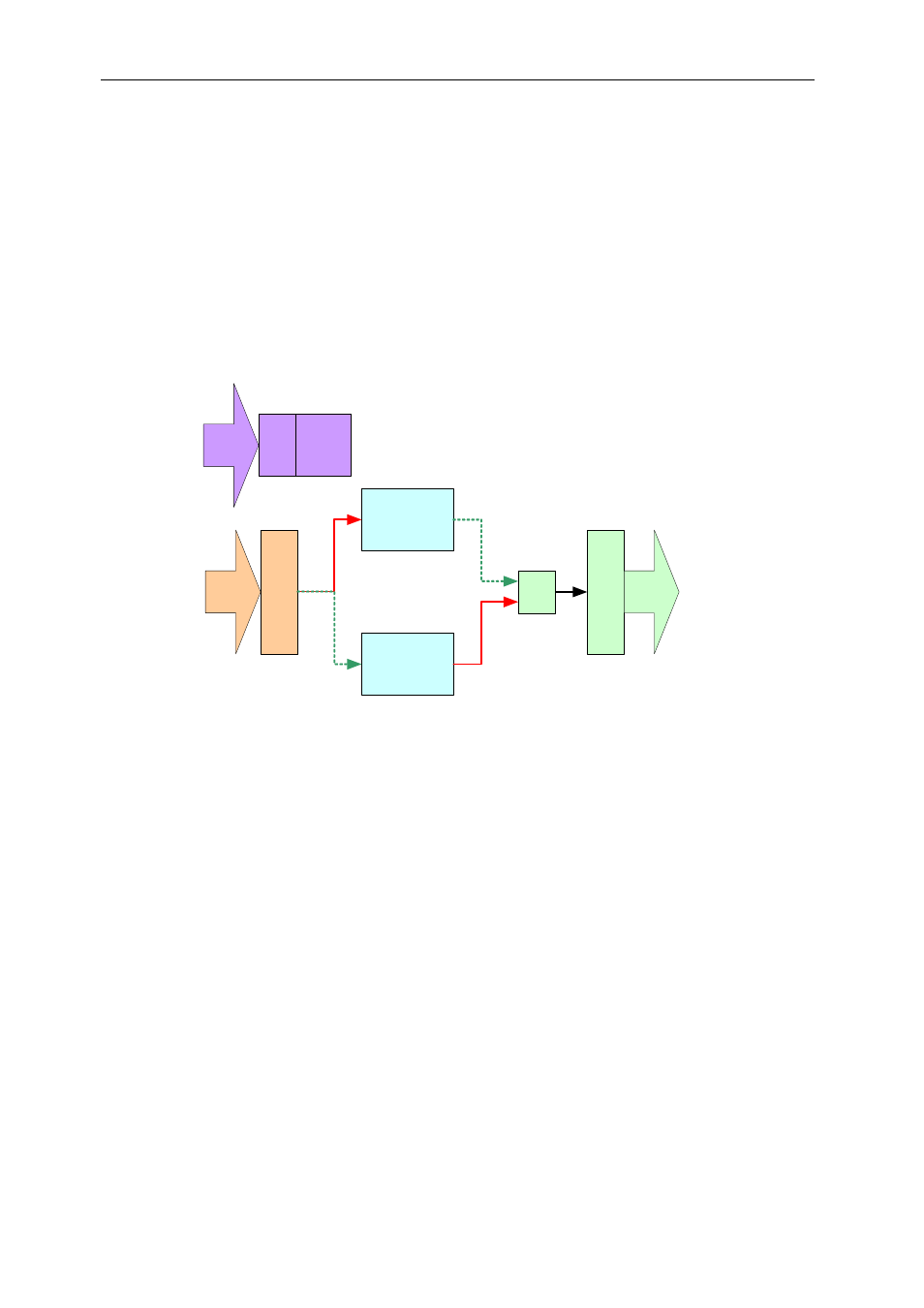
Functional description, Fpga design overview, Figure 2: smt351 fpga data flow – Sundance SMT351 User Manual
Page 14

Version 1.6
Page 14 of 25
SMT351 User Manual
Functional description
This section describes the functional architecture of the SMT351 programmed with
the release 2 of the firmware. This applies only to the boards shipped after the
01/08/06. The boards shipped before the 01/08/06 use the release 1 of the firmware
and you should refer to version 1.3 of the user manual. To upgrade from version 1 to
version 2 please contact Sundance.
FPGA design overview
The following diagram shows the data path implemented in the FPGA of the
SMT351:
SHB
A
SHB
B
Memory
compartment 0
Memory
compartment 1
Mux
400
MBytes/
sec
400
MBytes/
sec
Registers
Com
port
Control
words
Figure 2: SMT351 FPGA data flow.
Data input on SHB A are stored into memory and then sent to SHB B.
Memory is organised in two independent compartments: compartments 0 and
compartments 1.
Both compartments are accessed at the same time so that data can be stored in one
compartments while data are being read back from the other.
This mechanism allows a continuous data rate of 400MB/s.
This mechanism continues “repeat” times, where repeat is set by the user in the
“Repeat register”.
