Jp2 pinout, Figure 7: ttl i/os (jp2) pinout, Jp2: ttl i/os – Sundance SMT351 User Manual
Page 23: The following diagram shows jp2’s pinout
Version 1.6
Page 23 of 25
SMT351 User Manual
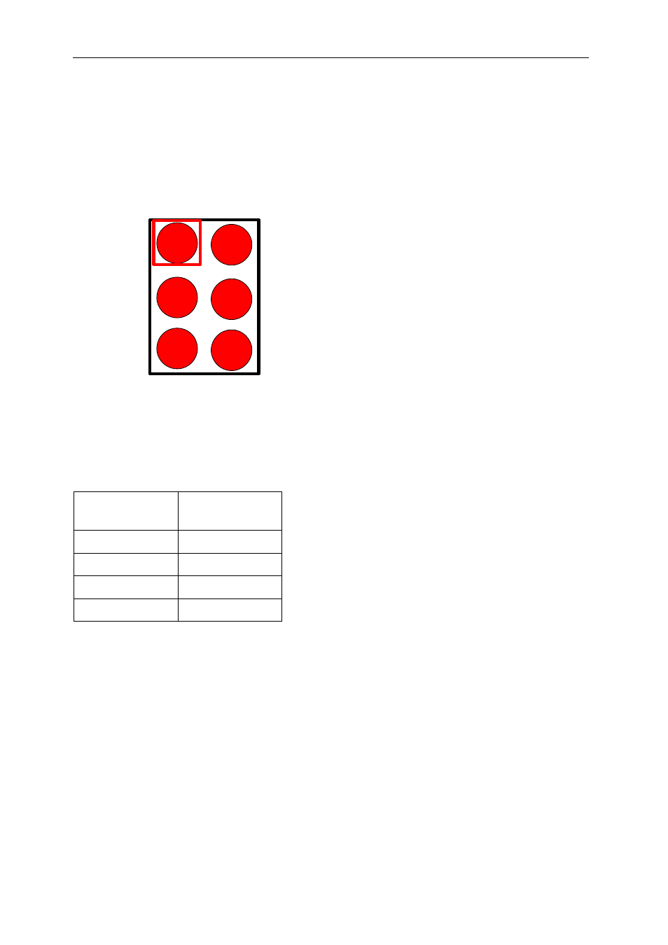
JP2 pinout
The following diagram shows JP2’s pinout:
2
TTL
0
4
TTL
2
6
GND
1
VCC
3
TTL
1
5
TTL
3
JP2: TTL I/Os
Figure 7: TTL I/Os (JP2) pinout
A square is drawn around pin 1 on PCB to indicate its location (Represented on
figure 5 in connectors location section).
The following table shows JP2 mapping to the FPGA:
Signal name
FPGA pin
number
TTL0 AC10
TTL1 AD10
TTL2 AC11
TTL3 AD11
See also other documents in the category Sundance Equipment:
- SMT107 (16 pages)
- SMT6035 v.2.2 (39 pages)
- SMT6012 v.4.6 (22 pages)
- FC100 (12 pages)
- FC108 v.1.1 (10 pages)
- SMT6065 v.4.0 (45 pages)
- FFT v.2.1 (19 pages)
- SMT111 (18 pages)
- SMT118LT (10 pages)
- SMT118 (20 pages)
- SMT123-SHB (13 pages)
- SMT128 (15 pages)
- SMT145 (18 pages)
- SMT148 (35 pages)
- SMT130 v.1.0 (46 pages)
- SMT148FX (48 pages)
- SMT310Q (55 pages)
- PARS (70 pages)
- SMT166-FMC (52 pages)
- SMT166 (44 pages)
- SMT300Q v.1.6 (61 pages)
- SMT310 v.1.6 (50 pages)
- SMT317 (24 pages)
- SMT326v2 (24 pages)
- SMT338 (19 pages)
- SMT349 (32 pages)
- SMT339 v.1.3 (27 pages)
- SMT338-VP (22 pages)
- SMT358 (25 pages)
- SMT351T (37 pages)
- SMT350 (45 pages)
- SMT362 (30 pages)
- SMT365G (23 pages)
- SMT364 (37 pages)
- SMT373 (15 pages)
- SMT368 (24 pages)
- SMT370v3 (46 pages)
- SMT377 (22 pages)
- SMT381 2007 (31 pages)
- SMT381-VP (81 pages)
- SMT387 (42 pages)
- SMT391 (18 pages)
- SMT384 (47 pages)
- SMT390-VP (55 pages)