Standoff locations – Measurement Computing USB-2627 User Manual
Page 28
USB-2627 User's Guide
Specifications
28
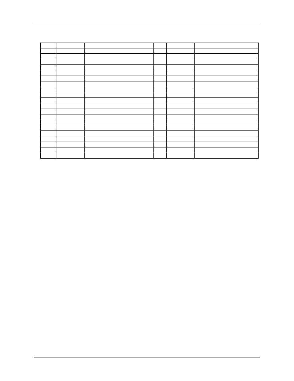
Table 24. J5 connector pinout
Pin
Signal name
Pin description
Pin
Signal name
Pin description
1
NC
No connection
2
NC
No connection
3
NC
No connection
4
NC
No connection
5
AGND
Analog ground
6
AGND
Analog ground
7
XDAC0
Analog output 0
8
XDAC2
Analog output 2
9
XDAC1
Analog output 1
10
XDAC3
Analog output 3
11
AGND
Analog ground
12
AGND
Analog ground
13
NC
No connection
14
AGND
Analog ground
15
AGND
Analog ground
16
AGND
Analog ground
17
TTLTRG
External digital trigger input
18
XDPCR
External analog output scan clock
19
XAPCR
External analog input scan clock
20
GND
Digital ground
21
GND
Digital ground
22
GND
Digital ground
23
NC
No connection
24
NC
No connection
25
+VO
Power output
26
NC
No connection
27
NC
No connection
28
NC
No connection
29
GND
Digital ground
30
NC
No connection
31
TMR2
Timer output 2
32
NC
No connection
33
GND
Digital ground
34
NC
No connection
35
TMR3
Timer output 3
36
NC
No connection
37
GND
Digital ground
38
NC
No connection
39
NC
No connection
40
NC
No connection
Standoff locations
The board is designed with standoff holes labeled TL1 to TL8.
TL1
: Standoff hole TL1 Is connected directly to the J1 USB connector shield.
TL2
: Standoff hole TL2 is connected directly to the P1 SCSI connector shield (pin 69, pin 70). The SCSI
connector shield and TL2 can also be connected to the board chassis ground guard trace using the R21
(OPEN by default) resistor location.
TL4-8
: Standoff holes TL4-TL8 are electrically isolated from the PCB.
Refer to the mechanical drawing in the hardware user guide for the location of these standoff holes.