2 a/d data & channel registers, 1 12-bit boards – Measurement Computing PC104-DAS16JR/12 User Manual
Page 16
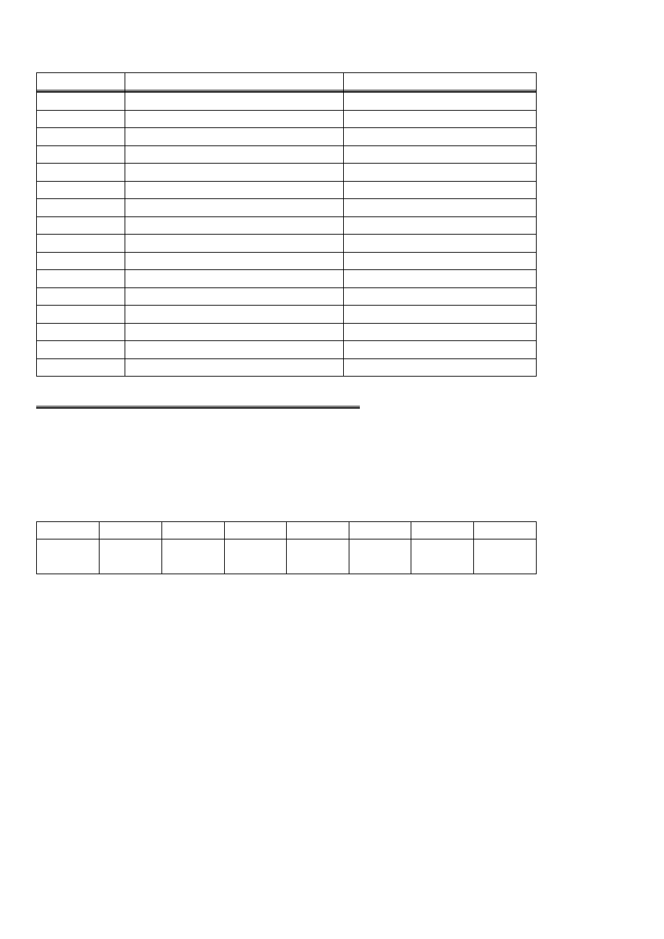
Table 3-2. Register Summary
Pacer Clock Control (8254)
None. No read back on 8254.
BASE + 15
CTR 2 Data - A/D Pacer
CTR 2 Data- A/D Pacer Clock
BASE + 14
CTR 1 Data - A/D Pacer
CTR 1 Data - A/D Pacer Clock
BASE + 13
Counter 0 Data
Counter 0 Data
BASE + 12
Gain control
Gain setting read-back
BASE + 11
None
Pacer clock control register
BASE + 10
Set DMA, INT etc.
DMA, Interrupt & Trigger Control
BASE + 9
None
Status EOC, UNI/BIP etc.
BASE + 8
None
None
BASE + 7
None
None
BASE + 6
None
None
BASE + 5
None
None
BASE + 4
Digital 4 Bit Output
Digital 4 Bit Input
BASE + 3
Channel MUX Set
Channel MUX Read
BASE + 2
None
A/D Bits 1 (MSB) to 8
BASE + 1
Start A/D Conversion
A/D Bits 9 to 12 (LSB) & Chan. #
BASE
WRITE FUNCTION
READ FUNCTION
ADDRESS
3.2 A/D DATA & CHANNEL REGISTERS
BASE ADDRESS:
3.2.1 12-BIT BOARDS
CH1
CH2
CH4
CH8
A/D12
LSB
A/D11
A/D10
A/D9
0
1
2
3
4
5
6
7
Read/write register.
READ
On read, it contains two types of data. The least significant four digits of the analog
input data and the channel number which the current data was taken from.
These four bits of analog input data must be combined with the eight bits of analog
input data in BASE + 1, forming a complete 12 bit number. The data is in the format
0 = minus full scale. 4095 = +FS.
The channel number is binary. The weights are shown in Table 3-1. If the current
channel were 5 then bits CH4 and CH1 would be high, CH8 and CH2 would be low.
12