Chapter 3 – DFI HM920-HM86 User Manual
Page 22
www.dfi .com
Chapter 3 Hardware Installation
22
Chapter 3
Signal
Pin#
Module Pin Type Pwr Rail /Tolerance
HM920
Carrier Board
Description
SPI_CS#
B97
O CMOS
3.3V Suspend/3.3V
Connect a series resistor 33ȟ to Carrier Board SPI Device CS# pin
Chip select for Carrier Board SPI - may be sourced from chipset SPI0 or SPI1
SPI_MISO
A92
I CMOS
3.3V Suspend/3.3V
Connect a series resistor 33ȟ to Carrier Board SPI Device SO pin
Data in to Module from Carrier SPI
SPI_MOSI
A95
O CMOS
3.3V Suspend/3.3V
Connect a series resistor 33ȟ to Carrier Board SPI Device SI pin
Data out from Module to Carrier SPI
SPI_CLK
A94
O CMOS
3.3V Suspend/3.3V
Connect a series resistor 33ȟ to Carrier Board SPI Device SCK pin
Clock from Module to Carrier SPI
SPI_POWER
A91
O
3.3V Suspend/3.3V
Power supply for Carrier Board SPI – sourced from Module – nominally
3.3V. The Module shall provide a minimum of 100mA on SPI_POWER.
Carriers shall use less than 100mA of SPI_POWER. SPI_POWER
shall only be used to power SPI devices on the Carrier
BIOS_DIS0#
A34
BIOS_DIS1#
B88
Signal
Pin#
Module Pin Type Pwr Rail /Tolerance
HM920
Carrier Board
Description
VGA_RED
B89
O Analog
Analog
PD 150 TO GND
PD 150R,connect to VGA connector with EMI filter & ESD protect component.
Red for monitor. Analog output
VGA_GRN
B91
O Analog
Analog
PD 150 TO GND
PD 150R,connect to VGA connector with EMI filter & ESD protect component.
Green for monitor. Analog output
VGA_BLU
B92
O Analog
Analog
PD 150 TO GND
PD 150R,connect to VGA connector with EMI filter & ESD protect component.
Blue for monitor. Analog output
VGA_HSYNC
B93
O CMOS
3.3V / 3.3V
Connect to VGA connector with a3.3V Buffer IC to isolate PCH & Display Device
Horizontal sync output to VGA monitor
VGA_VSYNC
B94
O CMOS
3.3V / 3.3V
Connect to VGA connector with a 33V Buffer IC to isolate PCH & Display Device
Vertical sync output to VGA monitor
VGA_I2C_CK
B95
I/O OD CMOS
3.3V / 3.3V
PU 2.2K TO 3.3V
Connect to VGA connector with a 3.3V to 5V Level shift circuit.
DDC clock line (I2C port dedicated to identify VGA monitor capabilities)
VGA_I2C_DAT
B96
I/O OD CMOS
3.3V / 3.3V
PU 2.2K TO 3.3V
Connect to VGA connector with a 3.3V to 5V Level shift circuit.
DDC data line.
Signal
Pin#
Module Pin Type Pwr Rail /Tolerance
HM920
Carrier Board
Description
IDE_D0
D7
IDE_D1
C10
IDE_D2
C8
IDE_D3
C4
IDE_D4
D6
IDE_D5
D2
IDE_D6
C3
IDE_D7
C2
IDE_D8
C6
IDE_D9
C7
IDE_D10
D3
IDE_D11
D4
IDE_D12
D5
IDE_D13
C9
IDE_D14
C12
IDE_D15
C5
IDE_A0
D13
IDE_A1
D14
IDE_A2
D15
IDE_IOW#
D9
O CMOS
3.3V / 3.3V
I/O write line to IDE device.
Data latched on trailing (rising) edge.
IDE_IOR#
C14
O CMOS
3.3V / 3.3V
I/O read line to IDE device.
IDE_REQ
D8
I CMOS
3.3V /5V
PU 5.6K TO GND
IDE Device DMA Request.
It is asserted by the IDE device to request a data transfer.
IDE_ACK#
D10
O CMOS
3.3V / 3.3V
IDE Device DMA Acknowledge.
IDE_CS1#
D16
O CMOS
3.3V / 3.3V
IDE Device Chip Select for 1F0h to 1FFh range.
IDE_CS3#
D17
O CMOS
3.3V / 3.3V
IDE Device Chip Select for 3F0h to 3FFh range.
IDE_IORDY
C13
I CMOS
3.3V /5V
PU 4.7K TO 3.3V
IDE device I/O ready input.
Pulled low by the IDE device to extend the cycle.
IDE_RESET#
D18
I/O CMOS
3.3V / 3.3V
Reset output to IDE device, active low.
IDE_IRQ
D12
I CMOS
3.3V /5V
PU 10K TO GND
Interrupt request from IDE device.
IDE_CBLID#
D77
I CMOS
3.3V /5V
PU 10K TO GND
Input from off-Module hardware indicating the type of IDE cable being
used. High indicates a 40-pin cable used for legacy IDE modes. Low
indicates that an 80-pin cable with interleaved grounds is used. Such a
cable is required for Ultra-DMA 66, 100 and 133 modes.
SPI Signals Descriptions
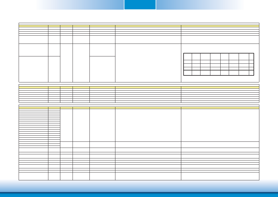
Selection straps to determine the BIOS boot device.
The Carrier should only float these or pull them low, please refer to
COM Express Module Base Specification Revision 2.1 for strapping options of BIOS disable signals.
VGA Signals Descriptions
NA
IDE Signals Descriptions
I CMOS
I/O CMOS
3.3V /5V
Bidirectional data to / from IDE device.
O CMOS
3.3V / 3.3V
Address lines to IDE device.
Ref
Line
Bios
Entry
SPI
Descriptor
Carrier
SPI_CS#
Chipset
SPI CS0#
Destination
Chipset
SPI CS1#
Destination
BIOS
DIS0#
BIOS
DIS1#
1
1
1
1
0
0
0
0
Module
Module
SPI0/SPI1
SPI1
(Default)
SPI0
High
High
Carrier
Carrier
Carrier
(Default)
Module
(Default)
Module
Module
Module
(Default)
Module
Module
Module
3
2
1
0
Carrier FWH
SPI0/SPI1
(Default)
SPI0/SPI1