Delta Electronics LCP-8500A4EDR User Manual
Page 5
LCP-8500A4EDR
Preliminary
DELTA ELECTRONICS, INC.
5 2008/7/16
Rev. 0A
www.deltaww.com
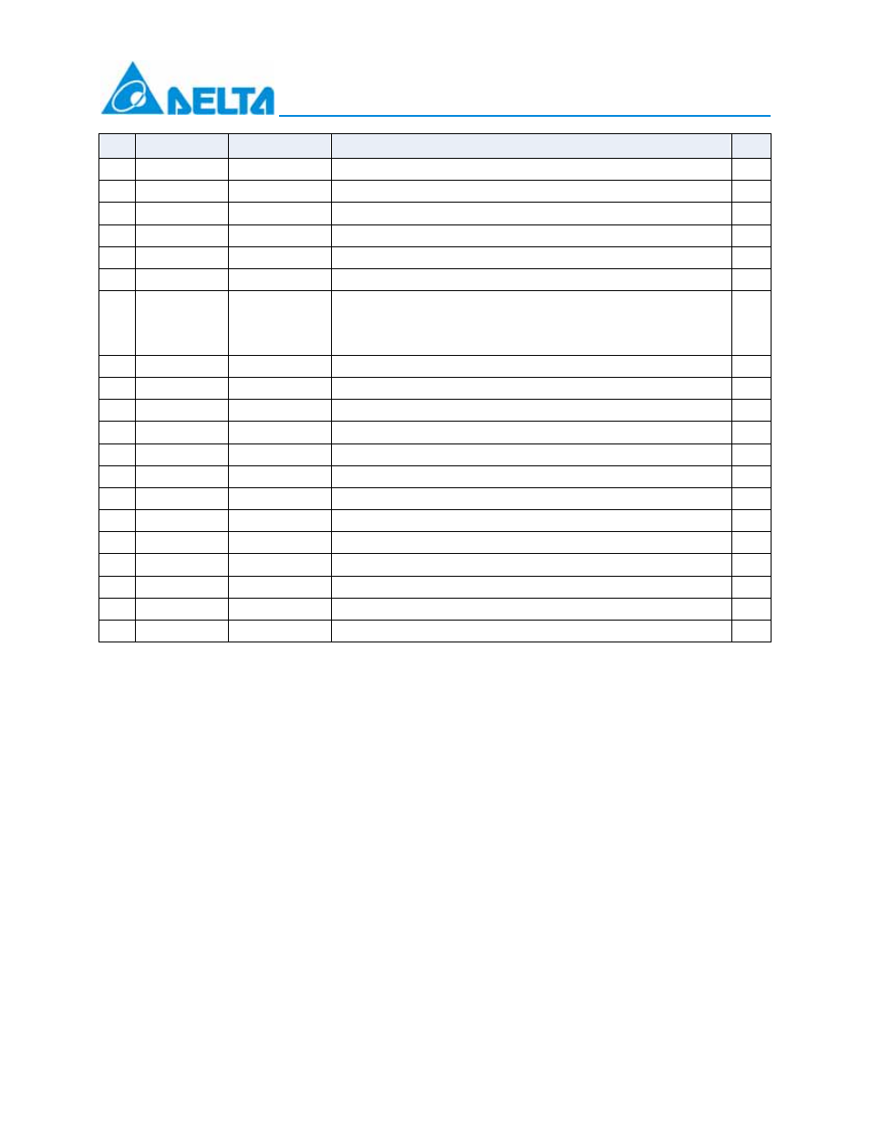
Pin
Logic
Symbol
Name/Description
Note
1
VeeT
Module Transmitter Ground
1
2
LVTTL-O
TX_Fault
Module Transmitter Fault
2
3
LVTTL-I
TX_Disable Transmitter Disable; Turns off transmitter laser output
3
4
LVTTL-I/O
SDA
2- write Serial Interface Data Line
5
LVTTL-I/O
SCL
2- write Serial Interface Clock
6
MOD_ABS Module Absent, connected to V
ee
T or V
ee
R in the module
4
7 LVTTL-I
RS0
Rate Select 0, optionally controls SFP+ module receiver.
When High input data rate>4.25GBd and when LOW input
data rate 4.25GBd.
8
LVTTL-O
RX_LOS
Receiver Loss of Signal Indication
2
9 LVTTL-I
RS1 Not
Implement
10
VeeR
Module Receiver Ground
1
11
VeeR
Module Receiver Ground
1
12
CML-O
RD-
Receiver Inverted Data Output
13
CML-O
RD+
Receiver Non-Inverter Data Output
14
VeeR
Module Receiver Ground
1
15
VccR
Module Receiver 3.3V Supply
16
VccT
Module Transmitter 3.3V Supply
17
VeeT
Module Transmitter Ground
1
18
CML-I
TD+
Transmitter Non-Inverted Data Input
19
CML-I
TD-
Transmitter Inverted Data Input
20
VeeT
Module Transmitter Ground
1
Notes:
1. The module signal ground pins, VeeR and VeeT, shall be isolated from the module case.
2. This pin is an open collector/drain output pin and shall be pulled up with 4.7k-10k ohms to Host_Vcc
on the host board. Pull ups can be connected to multiple power supplies, however the host board
design shall ensure that no module pin has voltage exceeding module VccT/R + 0.5V.
3. This pin is an open collector/drain input pin and shall be pulled up with 4.7k-10k ohms to VccT in the
Module.
4. This pin shall be pulled up with 4.7k-10k ohms to Host_Vcc on the host board.