At/ide interface connector jp1 – StorCase Technology DE75i-A100 User Manual
Page 22

DE75i-A100 User's Guide - Rev. D02
StorCase Technology, Inc.
Installation
15
AT/IDE Interface Connector JP1
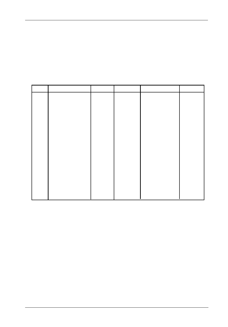
The AT/IDE Interface connector (JP1) pin assignments are as follows:
Table 2: AT/IDE Interface Signals
Pin
Signal
I/O
Pin
Signal
I/O
01
Host Reset-
O
02
Ground
03
Host Data 7
I/O
04
Host Data 8
I/O
05
Host Data 6
I/O
06
Host Data 9
I/O
07
Host Data 5
I/O
08
Host Data 10
I/O
09
Host Data 4
I/O
10
Host Data 11
I/O
11
Host Data 3
I/O
12
Host Data 12
I/O
13
Host Data 2
I/O
14
Host Data 13
I/O
15
Host Data 1
I/O
16
Host Data 14
I/O
17
Host Data 0
I/O
18
Host Data 15
I/O
19
Ground
20
Key
No Pin
21
Reserved
22
Ground
23
HIOW-
O
24
Ground
25
HIOR-
O
26
Ground
27
Reserved
28
Reserved
29
Reserved
30
Ground
31
IRQ 14
I
32
Host IO16-(AT)
I
33
Host ADDR 1
O
34
PDIAG- (16)
Notes
35
Host ADDR 0
O
36
Host ADDR 2
O
37
Host CS0-
O
38
Host CS1-
O
39
DASP-
Notes
40
Ground
- Indicates an active-low signal.
Signal direction is with respect to the host.
"I" indicates To the host
"O" indicates From the host
The PDIAG and DASP signals are used for communication between master and slave.
