3 pcb layout, 10 • installation – ADLINK ACL-8111 User Manual
Page 16

10
• Installation
2.3 PCB
Layout
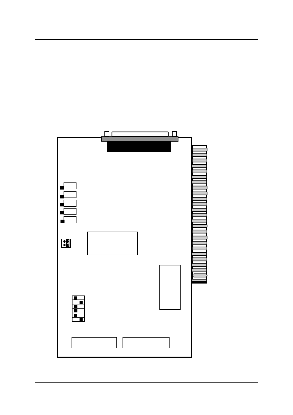
In ACL-8111, there are three connectors (CN1~CN3), one switch (SW1), one
jumper (JP1) and 5 variable resistors (VR1~VR5). Please refer Figure 2.3 to
identify the location these components.
The card's jumpers and switches are preset at the factory. Please setup the
switch and jumper according to the system setting and the application
requirements.
A jumper is closed (sometimes referred to as "shorted") with the plastic cap
inserted over two pins of the jumper. A jumper is open with the plastic cap
inserted over one or no pin(s) of the jumper.
CN1
VR
1
V
R
2
VR
3
V
R
4
SW
1
JP
1
JP
2
ADS57
4
81
11
-1
0
V
-5
V
VR
5
.
.
.
.
.
.
.
.
.
.
.
.
.
.
.
.
. .
. .
. .
. .
. .
. .
. .
. .
CN
2
CN
3
82
53
Figure 2.3 ACL-8111‘s PCB layout
See also other documents in the category ADLINK Hardware:
- USB-1901 (84 pages)
- USB-1210 (54 pages)
- USB-2401 (60 pages)
- USB-7230 (50 pages)
- USB-2405 (56 pages)
- DAQe-2010 (92 pages)
- DAQe-2204 (100 pages)
- DAQe-2213 (94 pages)
- DAQe-2501 (74 pages)
- PXI-2010 (84 pages)
- PXI-2020 (60 pages)
- PXI-2501 (62 pages)
- cPCI-9116 (98 pages)
- ACL-8112 Series (94 pages)
- ACL-8112 Series (92 pages)
- ACL-8112 Series (93 pages)
- ACL-8216 (75 pages)
- PCM-9112+ (10 pages)
- PCM-9112+ (94 pages)
- cPCI-6216V (47 pages)
- ACL-6126 (28 pages)
- ACL-6128A (40 pages)
- PCM-6308V+ (52 pages)
- PCM-6308V+ (4 pages)
- PCI-7444 (82 pages)
- PCI-7434 (48 pages)
- PCI-7234 (56 pages)
- PCI-7260 (66 pages)
- PCI-7258 (38 pages)
- PCI-7256 (48 pages)
- PCI-7250 (48 pages)
- LPCI-7250 (48 pages)
- PCI-7396 (65 pages)
- PCI-7296 (59 pages)
- PCI-8554 (67 pages)
- PCIe-7360 (94 pages)
- PCIe-7350 (86 pages)
- PCIe-7300A (114 pages)
- PCIe-7200 (51 pages)
- PCI-7300A (112 pages)
- PCI-7300A (83 pages)
- PCI-7200 (96 pages)
- cPCI-7300 (83 pages)
- cPCI-7300 (82 pages)
