ADLINK ACL-8112 Series User Manual
Page 55
Operation Theory
• 47
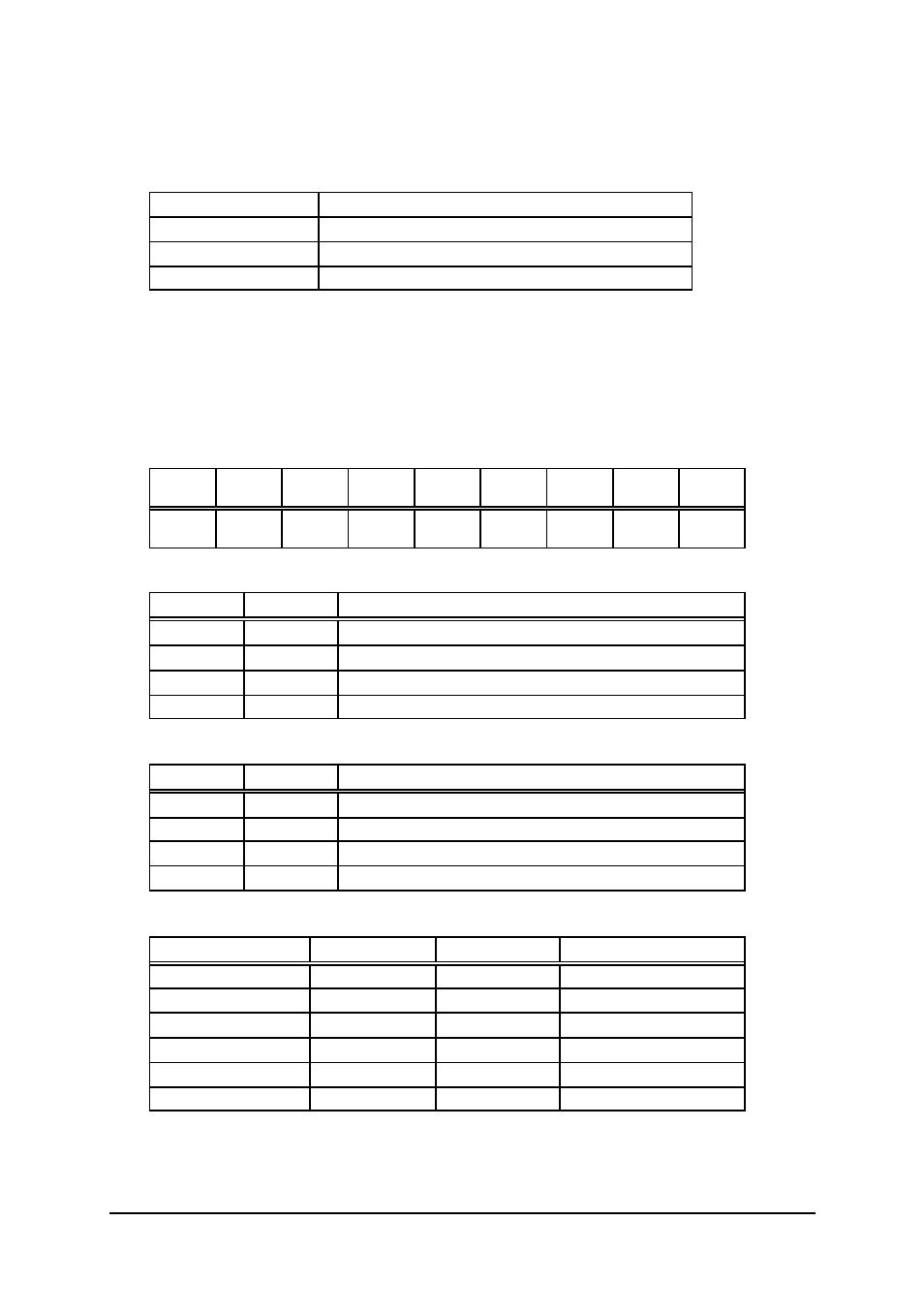
I/O Address
The 8254 in the ACL-8112 occupies 4 I/O address as shown below.
BASE + 0
LSB OR MSB OF COUNTER 0
BASE + 1
LSB OR MSB OF COUNTER 1
BASE + 2
LSB OR MSB OF COUNTER 2
BASE + 3
CONTROL BYTE
The programming of the 8254 is control by registers BASE+0 to BASE+3.
The function of each register is specified in this section. For more detailed
information, refer to the 8254 handbook.
Control Byte
Before loading or reading any of these individual counters, the control byte
(BASE+3) must be loaded first. The format of the control byte is:
Bit
7
6
5
4
3
2
1
0
SC1
SC0
RL1
RL0
M2
M1
M0
BCD
♦
SC1 & SC0 - Select Counter ( Bit7 & Bit 6)
SC1
SC0
COUNTER
0
0
Select Counter 0
0
1
Select Counter 1
1
0
Select Counter 2
1
1
ILLEGAL
♦
RL1 & RL0 - Select Read/Load operation ( Bit 5 & Bit 4)
RL1
RL0
OPERATION
0
0
COUNTER LATCH FOR STABLE READ
0
1
READ/LOAD LSB ONLY
1
0
READ/LOAD MSB ONLY
1
1
READ/LOAD LSB FIRST, THEN MSB
♦
M2, M1 & M0 - Select Operating Mode ( Bit 3, Bit 2, & Bit 1)
M2
M1
M0
MODE
0
0
0
0
0
0
1
1
x
1
0
2
x
1
1
3
1
0
0
4
1
0
1
5
♦
BCD - Select Binary/BCD Counting ( Bit 0)