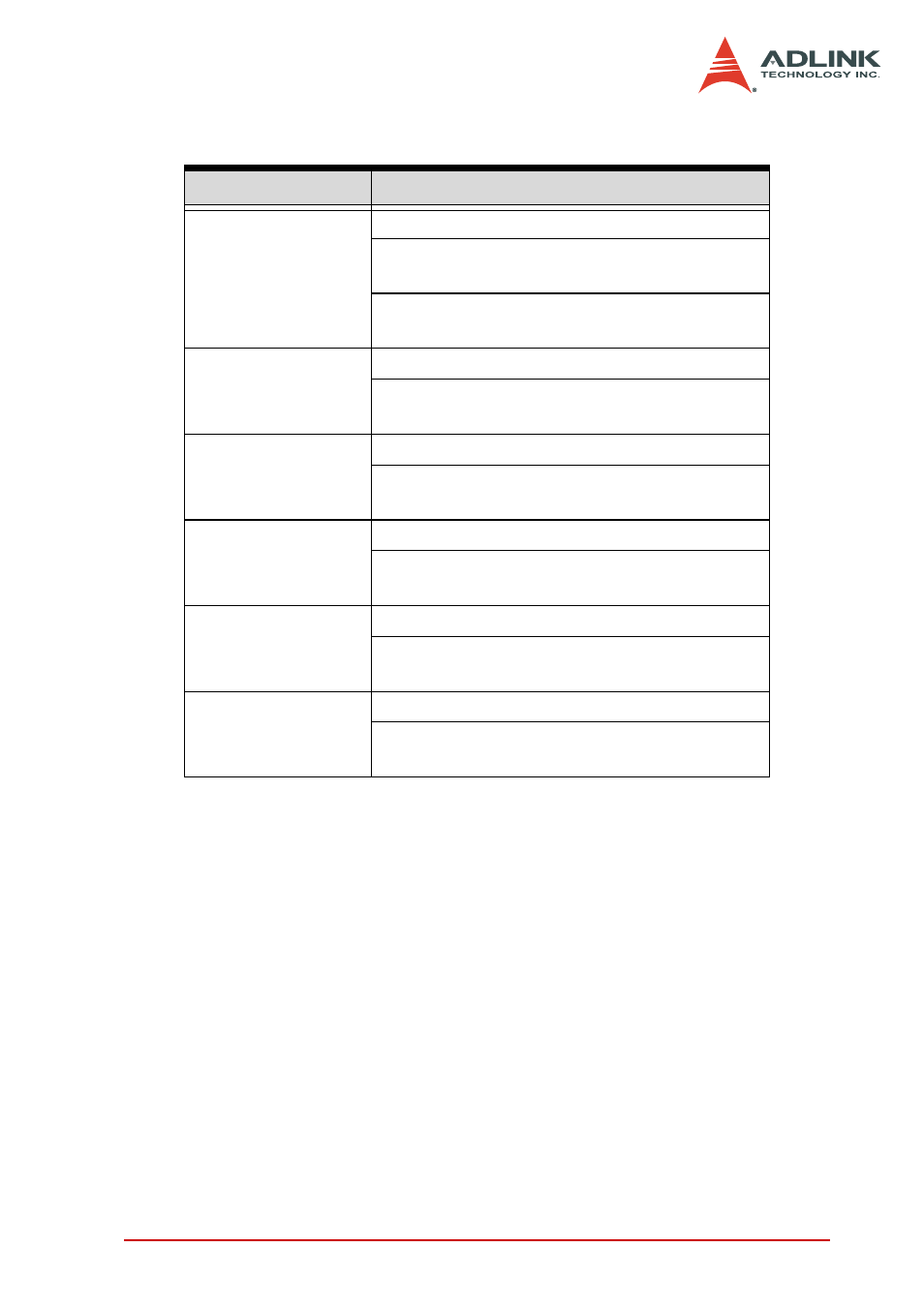
Table 4-10: ssi timing signals functionalities – ADLINK DAQe-2006 User Manual
Page 85
Operation Theory
73
In PCI form factor, there is a connector on the top right corner of
the card for the SSI. Refer to section 2.3 for the connector posi-
tion. All the SSI signals are routed to the 20-pin connector from the
FPGA. To synchronize multiple cards, users can connect a special
ribbon cable (ACL-SSI) to all the cards in a daisy-chain configura-
tion.
SSI timing signal
Functionality
SSI_TIMEBASE
SSI master: send the TIMEBASE out
SSI slave: accept the SSI_TIMEBASE to
replace the internal TIMEBASE signal.
Note: Affected on both A/D and D/A
operations
SSI_AD_TRIG
SSI master: send the internal AD_TRIG out
SSI slave: accept the SSI_AD_TRIG as the
digital trigger signal.
SSI_ADCONV
SSI master: send the ADCONV out
SSI slave: accept the SSI_ADCONV to
replace the internal ADCONV signal.
SSI_SCAN_START
SSI master: send the SCAN_START out
SSI slave: accept the SSI_SCAN_START to
replace the internal SCAN_START signal.
SSI_DA_TRIG
SSI master: send the DA_TRIG out.
SSI slave: accept the SSI_DA_TRIG as the
digital trigger signal.
SSI_DAWR
SSI master: send the DAWR out.
SSI slave: accept the SSI_DAWR to replace
the internal DAWR signal.
Table 4-10: SSI Timing Signals Functionalities