Table 4-1: bipolar analog input range and, Output digital code on daq/daqe/pxi-2010 – ADLINK DAQe-2006 User Manual
Page 43
Operation Theory
31
NOTE
Since the analog signal is sampled when an A/D conver-
sion starts (falling edge of A/D_conversion signal), while
SDI<1..0> are sam-pled right after an A/D conversion
completes (rising edge of nADBUSY signal). Precisely
SDI<1..0> are sampled within 220 to 400ns lag to the an-
alog signal, due to the variation of the conversion time of
the A/D converters.
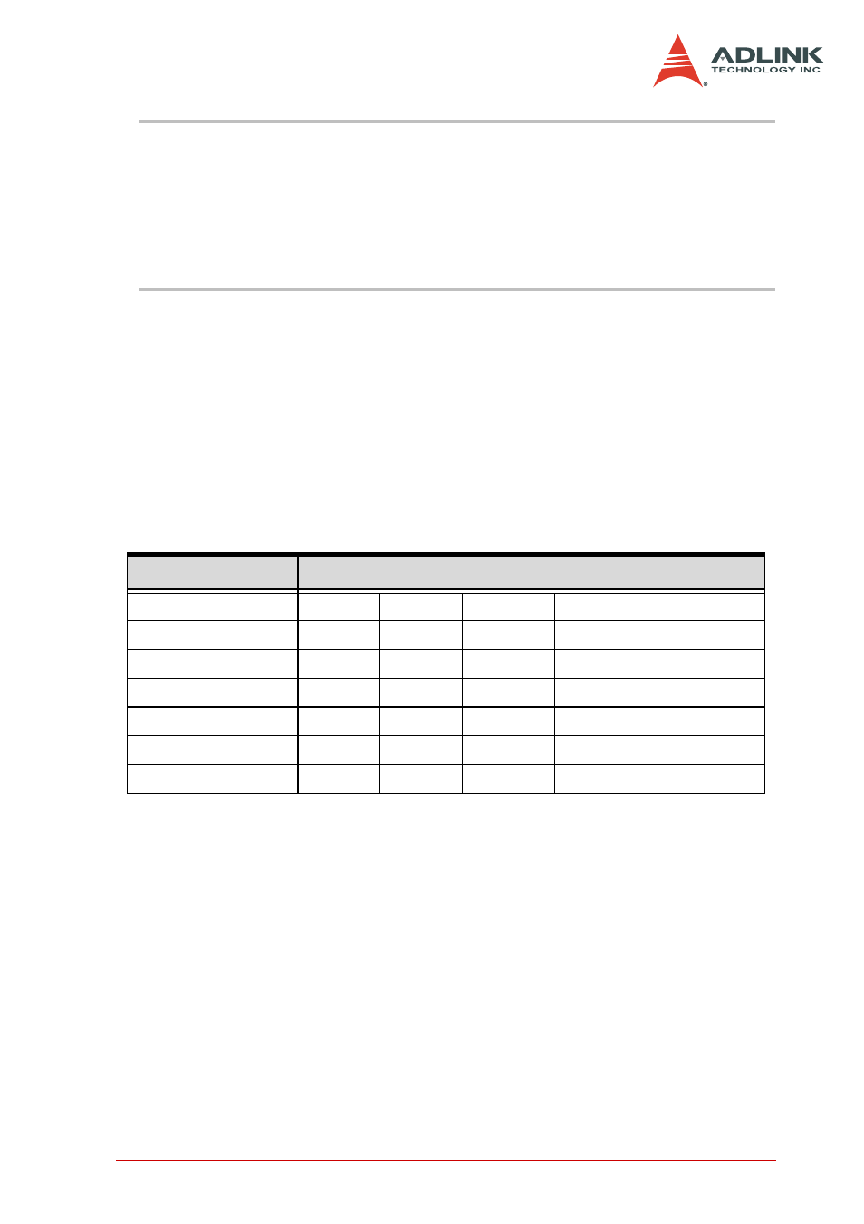
Table 4-1and Table 4-2 illustrate the ideal transfer characteristics
of various input ranges of DAQ/DAQe/PXI-2000/2010 Series card.
The converted digital codes for DAQ/DAQe/PXI-2010 are 14-bit
and 2’s complement, and here we present the codes as hexadeci-
mal numbers. Note that the last 2 bits of the transferred data,
which are the synchronous digital input (SDI), should be ignored
when retrieving the analog data, and that the last two digital codes
are SDI<1..0>)
Description
Bipolar Analog Input Range
Digital code
Full-scale Range
±10V
±5V
±2.5V
±1.25V
Least significant bit 1.22mV
0.61mV
0.305mV
0.153mV
FSR-1LSB
9.9988V 4.9994V
2.4997V
1.2499V
1FFF
Midscale +1LSB
1.22mV
0.61mV
0.305mV
0.153mV
0001
Midscale 0V
0V
0V
0V
0000
Midscale –1LSB
-1.22mV -0.61mV -0.305mV -0.153mV
3FFF
-FSR
-10V
-5V
-2.5V
-1.25V
2000
Table 4-1: Bipolar Analog Input Range and Output Digital Code on DAQ/
DAQe/PXI-2010