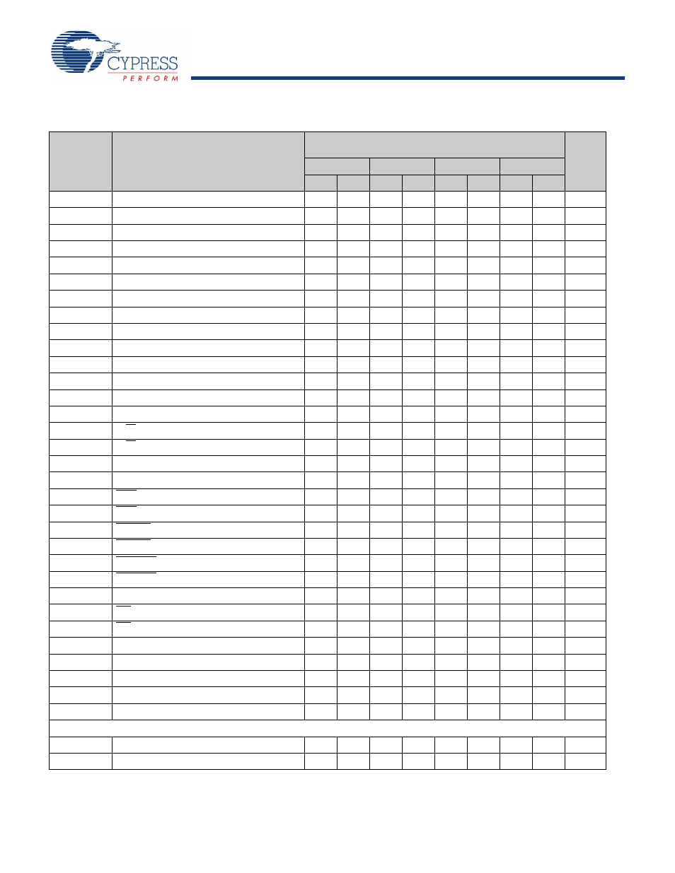
Switching characteristics over the operating range, Switching characteristics – Cypress CY7C09079V User Manual
Page 7

CY7C09079V/89V/99V
CY7C09179V/89V/99V
Document #: 38-06043 Rev. *C
Page 7 of 21
Notes
14. Test conditions used are Load 2.
15. This parameter is guaranteed by design, but it is not production tested.
Switching Characteristics
Over the Operating Range
Parameter
Description
CY7C09079V/89V/99V
CY7C09179V/89V/99V
Unit
-6
-7
-9
-12
Min
Max
Min
Max
Min
Max
Min
Max
f
MAX1
f
Max
Flow-Through
53
45
40
33
MHz
f
MAX2
f
Max
Pipelined
100
83
67
50
MHz
t
CYC1
Clock Cycle Time - Flow-Through
19
22
25
30
ns
t
CYC2
Clock Cycle Time - Pipelined
10
12
15
20
ns
t
CH1
Clock HIGH Time - Flow-Through
6.5
7.5
12
12
ns
t
CL1
Clock LOW Time - Flow-Through
6.5
7.5
12
12
ns
t
CH2
Clock HIGH Time - Pipelined
4
5
6
8
ns
t
CL2
Clock LOW Time - Pipelined
4
5
6
8
ns
t
R
Clock Rise Time
3
3
3
3
ns
t
F
Clock Fall Time
3
3
3
3
ns
t
SA
Address Set-Up Time
3.5
4
4
4
ns
t
HA
Address Hold Time
0
0
1
1
ns
t
SC
Chip Enable Set-Up Time
3.5
4
4
4
ns
t
HC
Chip Enable Hold Time
0
0
1
1
ns
t
SW
R/W Set-Up Time
3.5
4
4
4
ns
t
HW
R/W Hold Time
0
0
1
1
ns
t
SD
Input Data Set-Up Time
3.5
4
4
4
ns
t
HD
Input Data Hold Time
0
0
1
1
ns
t
SAD
ADS Set-Up Time
3.5
4
4
4
ns
t
HAD
ADS Hold Time
0
0
1
1
ns
t
SCN
CNTEN Set-Up Time
3.5
4.5
5
5
ns
t
HCN
CNTEN Hold Time
0
0
1
1
ns
t
SRST
CNTRST Set-Up Time
3.5
4
4
4
ns
t
HRST
CNTRST Hold Time
0
0
1
1
ns
t
OE
Output Enable to Data Valid
8
9
10
12
ns
t
OLZ
OE to Low Z
2
2
2
2
ns
t
OHZ
OE to High Z
1
7
1
7
1
7
1
7
ns
t
CD1
Clock to Data Valid - Flow-Through
15
18
20
25
ns
t
CD2
Clock to Data Valid - Pipelined
6.5
7.5
9
12
ns
t
DC
Data Output Hold After Clock HIGH
2
2
2
2
ns
t
CKHZ
Clock HIGH to Output High Z
2
9
2
9
2
9
2
9
ns
t
CKLZ
Clock HIGH to Output Low Z
2
2
2
2
ns
Port to Port Delays
t
CWDD
Write Port Clock HIGH to Read Data Delay
30
35
40
40
ns
t
CCS
Clock to Clock Set-Up Time
9
10
15
15
ns
