Software recall, Preventing store, Hardware protect – Cypress STK14C88-3 User Manual
Page 5: Noise considerations, Low average active power
STK14C88-3
Document Number: 001-50592 Rev. **
Page 5 of 17
Software RECALL
Data is transferred from the nonvolatile memory to the SRAM by
a software address sequence. A software RECALL cycle is
initiated with a sequence of READ operations in a manner similar
to the software STORE initiation. To initiate the RECALL cycle,
the following sequence of CE controlled READ operations is
performed:
1. Read address 0x0E38, Valid READ
2. Read address 0x31C7, Valid READ
3. Read address 0x03E0, Valid READ
4. Read address 0x3C1F, Valid READ
5. Read address 0x303F, Valid READ
6. Read address 0x0C63, Initiate RECALL cycle
Internally, RECALL is a two step procedure. First, the SRAM data
is cleared, and then the nonvolatile information is transferred into
the SRAM cells. After the t
RECALL
cycle time, the SRAM is once
again ready for READ and WRITE operations. The RECALL
operation does not alter the data in the nonvolatile elements. The
nonvolatile data can be recalled an unlimited number of times.
Preventing STORE
The STORE
function can be disabled on the fly by holding HSB
high with a driver capable of sourcing 30 mA at a V
OH
of at least
2.2V, because it has to overpower the internal pull down device.
This device drives HSB LOW for 20
μs at the onset of a STORE.
When the STK14C88-3 is connected for AutoStore operation
(system V
CC
connected to V
CC
and a 68
μF capacitor on V
CAP
)
and V
CC
crosses V
SWITCH
on the way down, the STK14C88-3
attempts to pull HSB LOW. If HSB does not actually get below
V
IL
, the part stops trying to pull HSB LOW and aborts the STORE
attempt.
Hardware Protect
The STK14C88-3 offers hardware protection against inadvertent
STORE operation and SRAM WRITEs during low voltage condi-
tions. When V
CAP
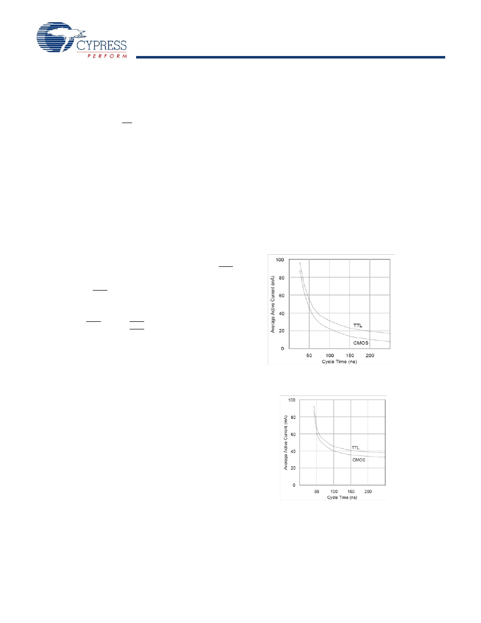
SWITCH , all externally initiated STORE operations and SRAM WRITEs are inhibited. Noise Considerations The STK14C88-3 is a high speed memory. It must have a high CC and V SS, using leads and traces that are as short as possible. As with all high speed CMOS ICs, careful routing of Low Average Active Power CMOS technology provides the STK14C88-3 the benefit of and show the relationship between I CC and READ or WRITE cycle time. Worst case current consumption is shown for both CMOS and TTL input levels 1. The duty cycle of chip enable 2. The overall cycle rate for accesses 3. The ratio of READs to WRITEs 4. CMOS versus TTL input levels 5. The operating temperature 6. The V CC level 7. IO loading Figure 4. Current Versus Cycle Time (READ) Figure 5. Current Versus Cycle Time (WRITE)
frequency bypass capacitor of approximately 0.1 µF connected
between V
power, ground, and signals reduce circuit noise.
drawing significantly less current when it is cycled at times longer
than 50 ns.
(commercial temperature range, VCC = 3.6V, 100% duty cycle
on chip enable). Only standby current is drawn when the chip is
disabled. The overall average current drawn by the STK14C88-3
depends on the following items: