Capacitance, Thermal resistance, Ac test loads and waveforms – Cypress CY7C1339G User Manual
Page 9: Electrical characteristics
CY7C1339G
Document #: 38-05520 Rev. *F
Page 9 of 18
I
SB3
Automatic CE
Power-down
Current—CMOS Inputs
V
DD
= Max, Device Deselected, or
V
IN
≤ 0.3V or V
IN
> V
DDQ
– 0.3V
f = f
MAX
= 1/t
CYC
4-ns cycle, 250 MHz
105
mA
5-ns cycle, 200 MHz
95
mA
6-ns cycle, 166 MHz
85
mA
7.5-ns cycle, 133 MHz
75
mA
I
SB4
Automatic CE
Power-down
Current—TTL Inputs
V
DD
= Max, Device Deselected,
V
IN
≥ V
IH
or V
IN
≤ V
IL
, f = 0
All Speeds
45
mA
Capacitance
[11]
Parameter
Description
Test Conditions
TQFP
Package
BGA
Package
Unit
C
IN
Input
Capacitance
T
A
= 25
°C, f = 1 MHz,
V
DD
= 3.3V.
V
DDQ
= 3.3V
5
5
pF
C
CLK
Clock Input Capacitance
5
5
pF
C
I/O
Input/Output Capacitance
5
7
pF
Thermal Resistance
[11]
Parameter
Description
Test Conditions
TQFP
Package
BGA
Package
Unit
Θ
JA
Thermal Resistance
(Junction to Ambient)
Test conditions follow standard test
methods and procedures for
measuring thermal impedance, per
EIA/JESD51
30.32
34.1
°C/W
Θ
JC
Thermal Resistance
(Junction to Case)
6.85
14.0
°C/W
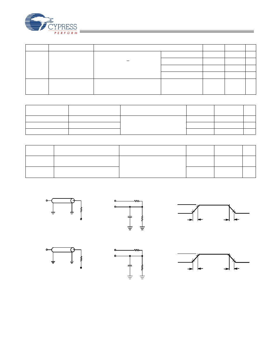
AC Test Loads and Waveforms
Note:
11. Tested initially and after any design or process change that may affect these parameters.
Electrical Characteristics
Over the Operating Range
[9, 10]
(continued)
Parameter
Description
Test Conditions
Min.
Max.
Unit
OUTPUT
R = 317
Ω
R = 351
Ω
5 pF
INCLUDING
JIG AND
SCOPE
(a)
(b)
OUTPUT
R
L
= 50
Ω
Z
0
= 50
Ω
V
T
= 1.5V
3.3V
ALL INPUT PULSES
V
DDQ
GND
90%
10%
90%
10%
≤ 1 ns
≤ 1 ns
(c)
OUTPUT
R = 1667
Ω
R = 1538
Ω
5 pF
INCLUDING
JIG AND
SCOPE
(a)
(b)
OUTPUT
R
L
= 50
Ω
Z
0
= 50
Ω
V
T
= 1.25V
2.5V
ALL INPUT PULSES
V
DDQ
GND
90%
10%
90%
10%
≤ 1 ns
≤ 1 ns
(c)
3.3V I/O Test Load
2.5V I/O Test Load
OUTPUT
R = 1667
Ω
R = 1538
Ω
5 pF
INCLUDING
JIG AND
SCOPE
(a)
(b)
OUTPUT
R
L
= 50
Ω
Z
0
= 50
Ω
V
T
= 1.25V
2.5V
ALL INPUT PULSES
V
DDQ
GND
90%
10%
90%
10%
≤ 1 ns
≤ 1 ns
(c)
2.5V I/O Test Load