Receiver dc offset calibration – Maxim Integrated 73M1866B/73M1966B Implementers Guide User Manual
Page 13
UG_1x66B_016
73M1866B/73M1966B Implementer’s Guide
Rev. 1.3
13
3.2.2 Receiver DC Offset Calibration
The effect of residual DC offset caused by the external components to the 73M1x66B can be reduced by
a simple procedure in which the magnitude of this DC offset is measured and subtracted from each
sample received from the PSTN. This calibration is intended to be performed once after power-on/reset
and is done only after the PLL is locked and the barrier is synchronized. The calibration can be
performed later if circumstances require intermittent calibration (for example if operating temperatures
vary drastically). The procedure can only be performed when the device is On-Hook.
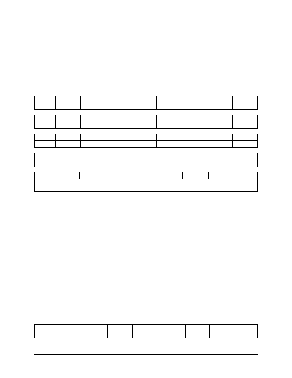
The registers used in this procedure are:
0x12
OFH
ENDC
ENAC
ENSHL
ENLVD
ENFEL
ENDT
ENNOM
Write
0
0
1
X
0
1
0
X
0x15
ENOLD
DISNTR
Res
CIDM
THEN
ENUVD
ENOVD
ENOID
Write
X
X
X
X
1
0
X
X
0x16
TXEN
RXEN
RLPEN
ATEN
ACZ3
ACZ2
ACZ1
ACZ0
Write
0
X
X
0
X
X
X
X
0x17
Res
Res
RXOCEN
Res
Res
Res
Res
Res
Write
X
X
1/0
X
X
X
X
X
0x25
RXOM7
RXOM6
RXOM5
RXOM4
RXOM3
RXOM2
RXOM1
RXOM0
Read/
Write
OFFSET
The temporary variables defined in this procedure are:
OFFSET = DC Offset value, RXOM[7:0].
Begin
1. Ensure that the device is On Hook (OFH==0). Executing the procedure when Off Hook will degrade
performance. If the device is Off Hook, return an error code indicating that the device cannot perform
the calibration routine.
2. Set ENDC,
ENLVD and ENDT to 0; set ENAC and ENFEL to 1 (write RG12 = x01x_010x2).
3. Set THEN to 1 and ENUVD to 0 (write RG15 = xxxx_10xx).
4. Set TXEN and ATEN to 0 (write RG16 = 0xx0_xxxx).
5. Set RXOCEN to 1 (write RG17 = xx1x_xxx).
6. Allow 1 second for the receive offset measurement to stabilize.
7. Set RXOCEN to 0 (write RG17 = xx0x_xxxx).
8. OFFSET = RXOM[7:0] (Read RG25).
9. Add 08h to OFFSET and write this result back into RXOM[7:0] (RG25 = OFFSET).
End
0x14
TXBST
DAA1
DAA0
Res
RXBST
RLPNH
RXG1
RXG0
Write
X
X
X
0
X
X
X
X