4 calibration, Calibration – Maxim Integrated MAXSANTAFEEVSYS User Manual
Page 11
MAXSANTAFEEVSYS User Manual
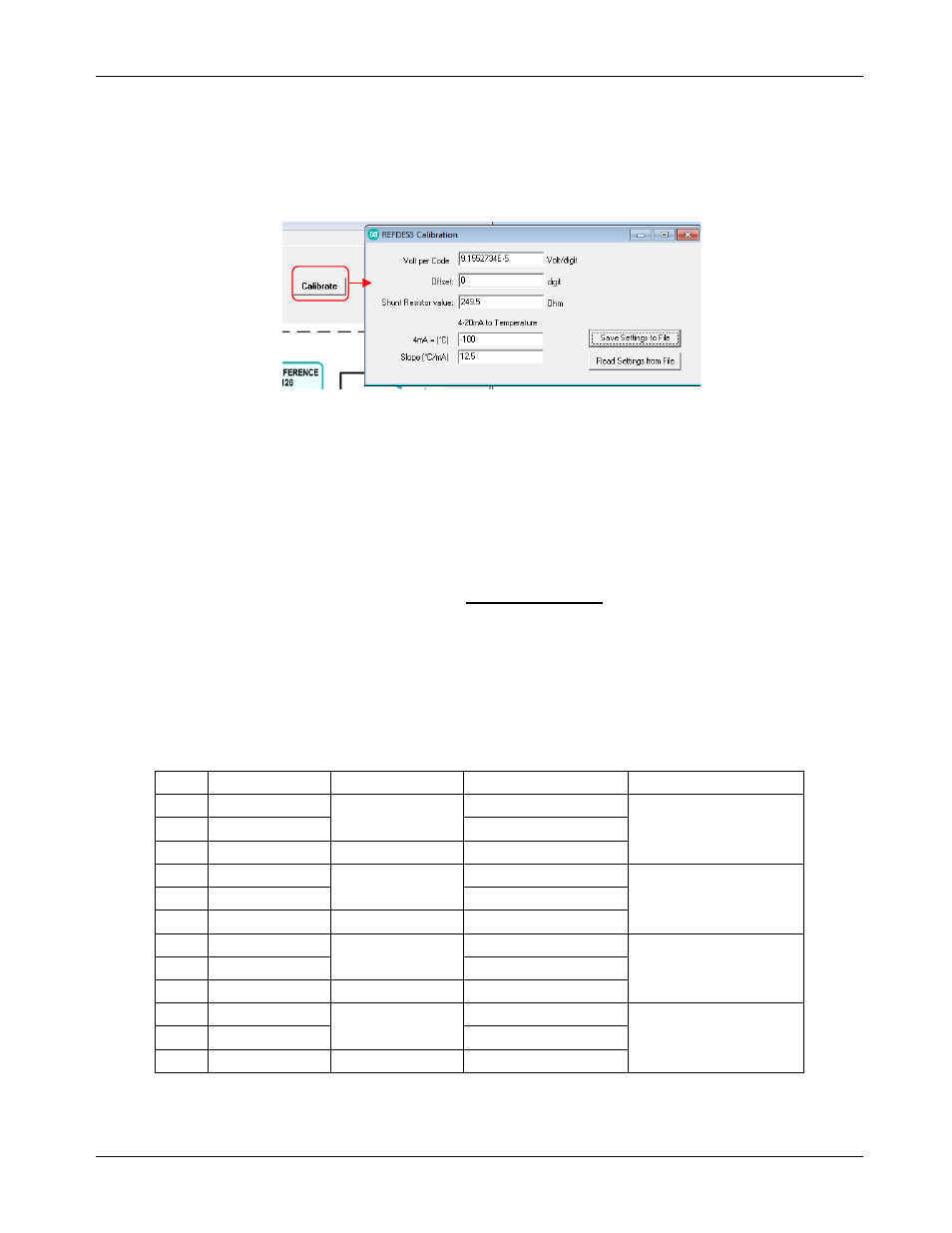
4.1.4 Calibration
For precision results, it is recommended to calibrate the MAXREFDES5 hardware using the function provided
with the GUI. Calibration parameters for each combination of input channel and input range are stored in a
local file in the GUI directory on the PC. Press the Calibration button to open a window with the calibration
parameters.
i. Save Settings to File: Saves the current settings to a local file on the PC. This should be done for
each valid combination of input channel and range (i.e. Input AIN0 with Input Range -12V to +12V).
ii. Offset: Offset calibration is done by forcing a 0V input voltage or 0mA current at the physical input.
The resulting plot counts value, if other than 0, should be entered in the offset digit tab of the
calibration window. Hit Tab on the keyboard for the value to be applied.
iii. Volt per Code: This option calibrates for gain error and should be adjusted after offset calibration.
The volt-per-code calibration is done by forcing a larger magnitude voltage at the input to obtain the
code. With the MAX5216DACLITE generator, this is limited to +3V (for best results with the max 3V
output, move the jumper wire from OUT of J5 to VREF of J4). Hit Tab on the keyboard for the value
to be applied.
Volt per code =
𝑉
𝐹𝑢𝑙𝑙𝑆𝑐𝑎𝑙𝑒 𝐼𝑛𝑝𝑢𝑡 𝑅𝑎𝑛𝑔𝑒
2
16
−1
iv. Read Settings from File: Reads the last settings that are in the file and returns the user to the input
and calibration values from the last saved settings. If one wishes to reset to factory default, then the
appropriate .ini file has to be deleted.
v. Shunt Resistor value: This option stores the exact value of shunt resistance of the board. This
optional field allows the user to change the resistance and scale the current measured.
Example Calibration Sequence:
STEP
DESCRIPTION
CONNECTIONS
DACLITE GUI
REFDES5 GUI
1
AIN0 Offset Cal
J5:OUT to AIN0
J5:GND to GND0
Single Operation: 0V
AIN0 with -12V to +12V
Input Range Selected
2
AIN0 Gain Cal
Single Operation: 2.5V
3
Save Settings
--
--
4
AIN1 Offset Cal
J5:OUT to AIN1
J5:GND to GND1
Single Operation: 0V
AIN1 with -12V to +12V
Input Range Selected
5
AIN1 Gain Cal
Single Operation: 2.5V
6
Save Settings
--
--
7
AIN2 Offset Cal
J5:OUT to AIN2
J5:GND to GND2
Single Operation: 0V
AIN2 with 0V to +6V
Input Range Selected
8
AIN2 Gain Cal
Single Operation: 2.5V
9
Save Settings
--
--
10
AIN3 Offset Cal
J5:OUT to AIN3
J5:GND to GND3
Single Operation: 0V
AIN3 with 0V to +12V
Input Range Selected
11
AIN3 Gain Cal
Single Operation: 2.5V
12
Save Settings
--
--
Rev 0
11