Cypress CY7C1347G User Manual
Page 7
CY7C1347G
Document #: 38-05516 Rev. *F
Page 7 of 22
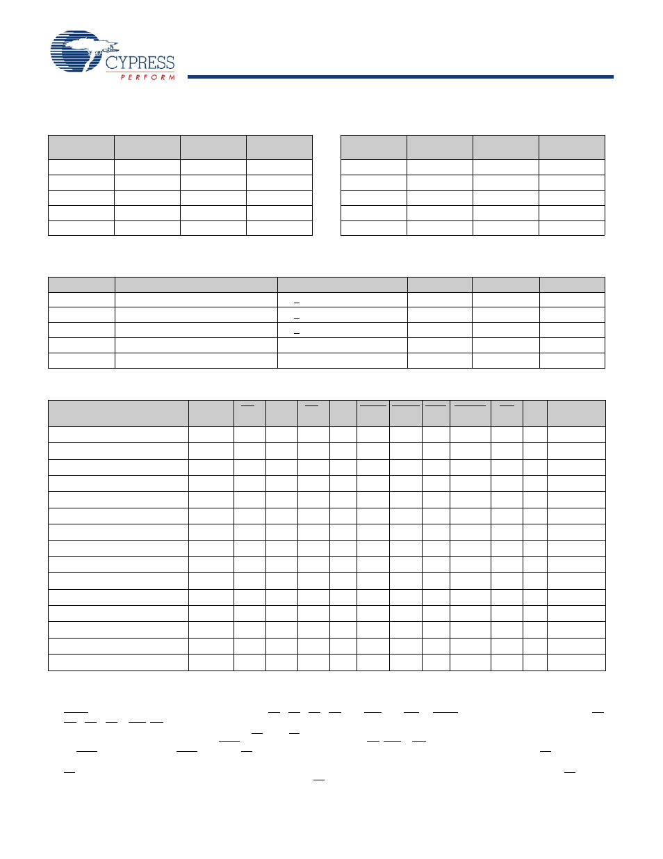
Table 2. Interleaved Burst Sequence
First
Address
Second
Address
Third
Address
Fourth
Address
A
[1:0]
A
[1:0]
A
[1:0]
A
[1:0]
00
01
10
11
01
00
11
10
10
11
00
01
11
10
01
00
Table 3. Linear Burst Sequence
First
Address
Second
Address
Third
Address
Fourth
Address
A
[1:0]
A
[1:0]
A
[1:0]
A
[1:0]
00
01
10
11
01
10
11
00
10
11
00
01
11
00
01
10
Table 4. ZZ Mode Electrical Characteristics
Parameter
Description
Test Conditions
Min
Max
Unit
I
DDZZ
Snooze mode standby current
ZZ > V
DD
− 0.2V
40
mA
t
ZZS
Device operation to ZZ
ZZ > V
DD
− 0.2V
2t
CYC
ns
t
ZZREC
ZZ recovery time
ZZ < 0.2V
2t
CYC
ns
t
ZZI
ZZ Active to snooze current
This parameter is sampled
2t
CYC
ns
t
RZZI
ZZ Inactive to exit snooze current
This parameter is sampled
0
ns
Table 5. Truth Table
Next Cycle
Add.
Used
CE
1
CE
2
CE
3
ZZ
ADSP ADSC ADV WRITE
OE
CLK
DQ
Deselect Cycle, Power Down
None
H
X
X
L
X
L
X
X
X
L-H Tri-State
Deselect Cycle, Power Down
None
L
L
X
L
L
X
X
X
X
L-H Tri-State
Deselect Cycle, Power Down
None
L
X
H
L
L
X
X
X
X
L-H Tri-State
Deselect Cycle, Power Down
None
L
L
X
L
H
L
X
X
X
L-H Tri-State
Deselect Cycle, Power Down
None
L
X
H
L
H
L
X
X
X
L-H Tri-State
Snooze Mode, Power Down
None
X
X
X
H
X
X
X
X
X
X
Tri-State
Read Cycle, Begin Burst
External
L
H
L
L
L
X
X
X
L
L-H Q
Read Cycle, Begin Burst
External
L
H
L
L
L
X
X
X
H
L-H Tri-State
Write Cycle, Begin Burst
External
L
H
L
L
H
L
X
L
X
L-H D
Read Cycle, Begin Burst
External
L
H
L
L
H
L
X
H
L
L-H Q
Read Cycle, Begin Burst
External
L
H
L
L
H
L
X
H
H
L-H Tri-State
Read Cycle, Continue Burst
Next
X
X
X
L
H
H
L
H
H
L-H Tri-State
Read Cycle, Continue Burst
Next
X
X
X
L
H
H
L
H
L
L-H Q
Read Cycle, Continue Burst
Next
H
X
X
L
X
H
L
H
L
L-H Q
Read Cycle, Continue Burst
Next
H
X
X
L
X
H
L
H
H
L-H Tri-State
Note
2. X = “Do Not Care.” H = Logic HIGH, L = Logic LOW.
3. WRITE = L when any one or more Byte Write Enable signals (BW
A
, BW
B
, BW
C
, BW
D
) and BWE = L or GW = L. WRITE = H when all Byte Write Enable signals (BW
A
,
BW
B
, BW
C
, BW
D
), BWE, GW = H.
4. The DQ pins are controlled by the current cycle and the OE signal. OE is asynchronous and is not sampled with the clock.
5. The SRAM always initiates a read cycle when ADSP is asserted, regardless of the state of GW, BWE, or BW
[A:D]
. Writes may occur only on subsequent clocks after
the ADSP or with the assertion of ADSC. As a result, OE must be driven HIGH before the start of the write cycle to allow the outputs to tri-state. OE is a don't care for
the remainder of the write cycle.
6. OE is asynchronous and is not sampled with the clock rise. It is masked internally during write cycles. During a read cycle all data bits are tri-state when OE is inactive
or when the device is deselected, and all data bits behave as output when OE is active (LOW).