Maximum ratings, Operating range, Electrical characteristics – Cypress CY7C1381DV25 User Manual
Page 17
CY7C1381DV25, CY7C1381FV25
CY7C1383DV25, CY7C1383FV25
Document #: 38-05547 Rev. *E
Page 17 of 28
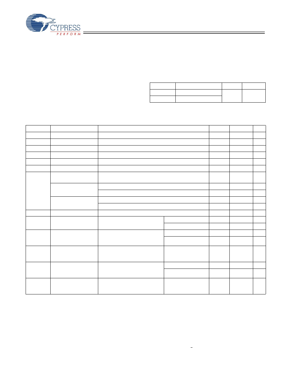
Maximum Ratings
Exceeding the maximum ratings may impair the useful life of
the device. For user guidelines, not tested.
Storage Temperature ................................. –65°C to +150°C
Ambient Temperature with
Power Applied............................................. –55°C to +125°C
Supply Voltage on V
DD
Relative to GND ....... –0.3V to +3.6V
Supply Voltage on V
DDQ
Relative to GND ...... –0.3V to +V
DD
DC Voltage Applied to Outputs
in Tri-State........................................... –0.5V to V
DDQ
+ 0.5V
DC Input Voltage ................................... –0.5V to V
DD
+ 0.5V
Current into Outputs (LOW) ........................................ 20 mA
Static Discharge Voltage.......................................... > 2001V
(per MIL-STD-883, Method 3015)
Latch-up Current ................................................... > 200 mA
Operating Range
Range
Ambient Temperature
V
DD
V
DDQ
Commercial
0°C to +70°C
2.5V
± 5% 2.5V – 5%
to V
DD
Industrial
–40°C to +85°C
Electrical Characteristics
Over the Operating Range
Parameter
Description
Test Conditions
Min.
Max.
Unit
V
DD
Power Supply Voltage
2.375
2.625
V
V
DDQ
IO Supply Voltage
for 2.5V IO
2.375
V
DD
V
V
OH
Output HIGH Voltage
for 2.5V IO, I
OH
= –1.0 mA
2.0
V
V
OL
Output LOW Voltage
for 2.5V IO, I
OL
= 1.0 mA
0.4
V
V
IH
Input HIGH Voltage
for 2.5V IO
1.7
V
DD
+ 0.3V
V
V
IL
Input LOW Voltage
for 2.5V IO
–0.3
0.7
V
I
X
Input Leakage Current
except ZZ and MODE
GND
≤ V
I
≤ V
DDQ
–5
5
µA
Input Current of MODE Input = V
SS
–30
µA
Input = V
DD
5
µA
Input Current of ZZ
Input = V
SS
–5
µA
Input = V
DD
30
µA
I
OZ
Output Leakage Current GND
≤ V
I
≤ V
DD,
Output Disabled
–5
5
µA
I
DD
V
DD
Operating Supply
Current
V
DD
= Max., I
OUT
= 0 mA,
f = f
MAX
= 1/t
CYC
7.5-ns cycle, 133 MHz
210
mA
10-ns cycle, 100 MHz
175
mA
I
SB1
Automatic CE
Power Down
Current—TTL Inputs
Max. V
DD
, Device Deselected,
V
IN
≥ V
IH
or V
IN
≤ V
IL
, f = f
MAX,
inputs switching
7.5-ns cycle, 133 MHz
140
mA
10-ns cycle, 100 MHz
120
I
SB2
Automatic CE
Power Down
Current—CMOS Inputs
Max. V
DD
, Device Deselected,
V
IN
≥ V
DD
– 0.3V or V
IN
≤ 0.3V,
f = 0, inputs static
All speeds
70
mA
I
SB3
Automatic CE
Power Down
Current—CMOS Inputs
Max. V
DD
, Device Deselected,
V
IN
≥ V
DDQ
– 0.3V or V
IN
≤ 0.3V,
f = f
MAX
, inputs switching
7.5-ns cycle, 133 MHz
130
mA
10-ns cycle, 100 MHz
110
mA
I
SB4
Automatic CE
Power Down
Current—TTL Inputs
Max. V
DD
, Device Deselected,
V
IN
≥ V
DD
– 0.3V or V
IN
≤ 0.3V,
f = 0, inputs static
All speeds
80
mA
Notes
16. Overshoot: V
IH
(AC) < V
DD
+1.5V (Pulse width less than t
CYC
/2), undershoot: V
IL
(AC) > –2V (Pulse width less than t
CYC
/2).
17. T
power up
: assumes a linear ramp from 0V to V
DD
(min.) within 200 ms. During this time V
IH
< V
DD
and V
DDQ
< V
DD
.