Switching waveforms – Cypress CY7C1319CV18 User Manual
Page 26
CY7C1317CV18, CY7C1917CV18
CY7C1319CV18, CY7C1321CV18
Document Number: 001-07161 Rev. *D
Page 26 of 31
Switching Waveforms
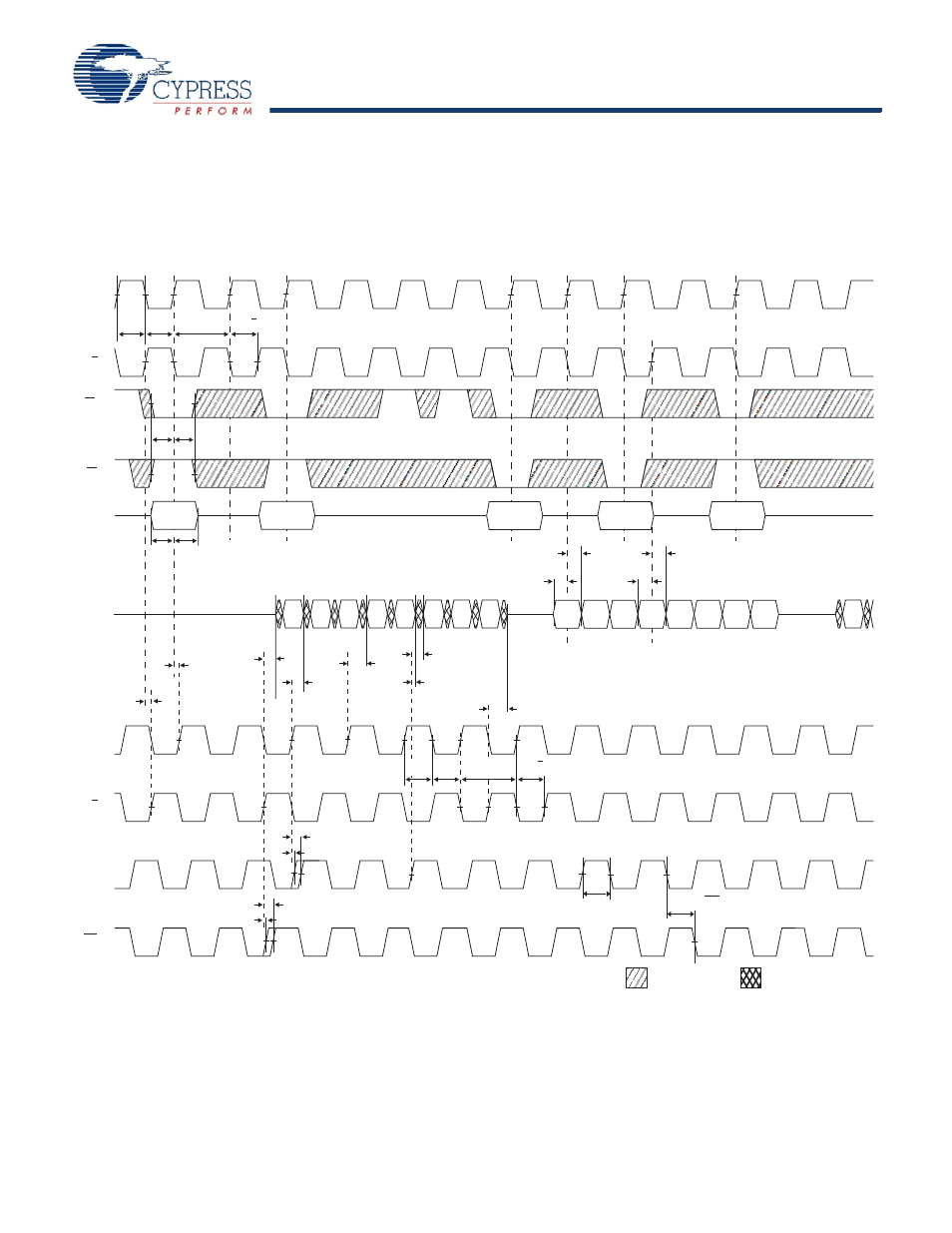
Figure 5. Read/Write/Deselect Sequence
K
1
2
3
4
5
6
7
8
9
10
11
12
13
A
DQ
C
READ
(burst of 4)
READ
(burst of 4)
READ
(burst of 4)
NOP
NOP
WRITE
(burst of 4)
WRITE
(burst of 4)
NOP
DON’T CARE
UNDEFINED
CQ
K
LD
R/W
C
CQ
tKH tKL
tCYC
tKHKH
tSC tHC
tSA tHA
A0
A1
A2
A3
A4
Q00
Q01
Q02
Q03
Q10
Q11
Q12
Q13
D20
D21
D22
D23
D30
D31
D32
D33
tHD
tSD
tHD
tSD
tKHCH
tKHCH
tCLZ
tDOH
tCO
tCQD
tCQDOH
tCHZ
tCCQO
tKH tKL
tCYC tKHKH
tCQOH
tCCQO
tCQOH
tCQHCQH
tCQH
Q40
Notes
27. Q00 refers to output from address A0. Q01 refers to output from the next internal burst address following A0, that is, A0 + 1.
28. Outputs are disabled (High-Z) one clock cycle after a NOP.
29. In this example, if address A4 = A3, then data Q40 = D30, Q41 = D31, Q42 = D32, and Q43 = D43. Write data is forwarded immediately as read results. This note
applies to the whole diagram.