Application example, Truth table – Cypress CY7C1319CV18 User Manual
Page 10
CY7C1317CV18, CY7C1917CV18
CY7C1319CV18, CY7C1321CV18
Document Number: 001-07161 Rev. *D
Page 10 of 31
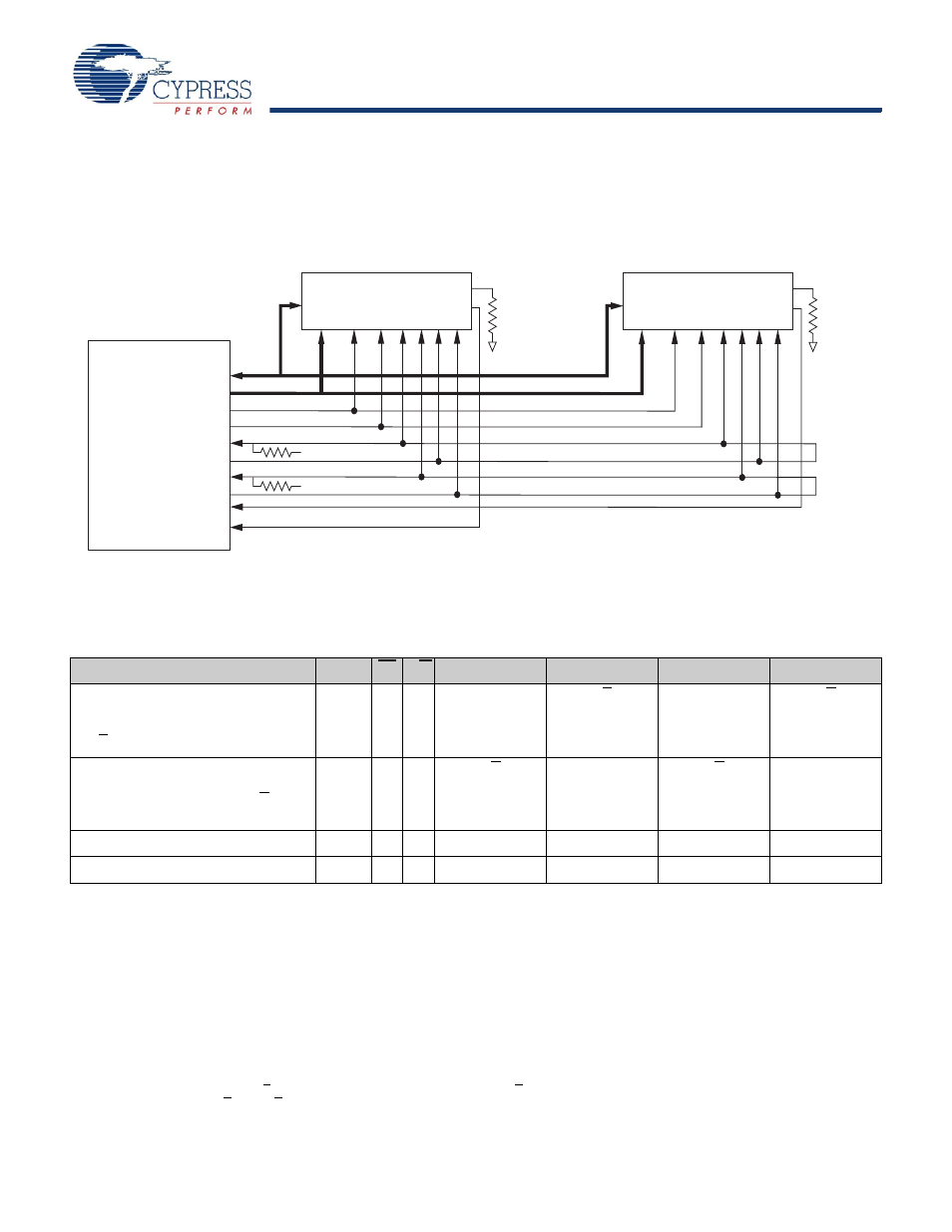
Application Example
shows two DDR-II used in an application.
Figure 1. Application Example
Truth Table
The truth table for the CY7C1317CV18, CY7C1917CV18, CY7C1319CV18, and CY7C1321CV18 follows.
Operation
K
LD R/W
DQ
DQ
DQ
DQ
Write Cycle:
Load address; wait one cycle;
input write data on four consecutive K
and K rising edges.
L-H
L
L
D(A1) at K(t + 1)
↑ D(A2) at K(t + 1)↑ D(A3) at K(t + 2)↑ D(A4) at K(t + 2)↑
Read Cycle:
Load address; wait one and a half cycle;
read data on four consecutive C and C
rising edges.
L-H
L
H Q(A1) at C(t + 1)
↑ Q(A2) at C(t + 2)↑ Q(A3) at C(t + 2)↑ Q(A4) at C(t + 3)↑
NOP: No Operation
L-H
H
X High-Z
High-Z
High-Z
High-Z
Standby: Clock Stopped
Stopped
X
X Previous State
Previous State
Previous State
Previous State
Vterm = 0.75V
Vterm = 0.75V
R = 50
ohms
R = 250
ohms
LD#
C C#
R/W#
DQ
A
K
LD#
C C#
R/W#
DQ
A
K
SRAM#1
SRAM#2
R
= 250ohms
BUS
MASTER
(CPU
or
ASIC)
DQ
Addresses
Cycle Start#
R/W#
Return CLK
Source CLK
Return CLK#
Source CLK#
Echo Clock1/Echo Clock#1
Echo Clock2/Echo Clock#2
ZQ
CQ/CQ#
K#
ZQ
CQ/CQ#
K#
Notes
2. X = “Don’t Care,” H = Logic HIGH, L = Logic LOW,
↑
represents rising edge.
3. Device powers up deselected with the outputs in a tri-state condition.
4. On CY7C1319CV18 and CY7C1321CV18, “A1” represents address location latched by the devices when transaction was initiated and “A2”, “A3”, “A4” represents the
addresses sequence in the burst. On CY7C1317CV18 and CY7C1917CV18, “A1” represents A + ‘00’ and “A2” represents A + ‘01’, “A3” represents A + ‘10’ and “A4”
represents A + ‘11’.
5. “t” represents the cycle at which a read/write operation is started. t + 1 and t + 2 are the first and second clock cycles succeeding the “t” clock cycle.
6. Data inputs are registered at K and K rising edges. Data outputs are delivered on C and C rising edges, except when in single clock mode.
7. It is recommended that K = K and C = C = HIGH when clock is stopped. This is not essential, but permits most rapid restart by overcoming transmission line charging
symmetrically.