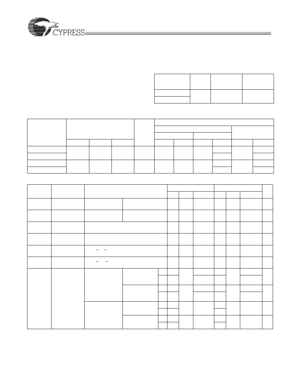
Maximum ratings, Operating range, Product portfolio – Cypress CY62147DV18 User Manual
Page 3

CY62147DV18
MoBL2™
Document #: 38-05343 Rev. *B
Page 3 of 11
Maximum Ratings
(Above which the useful life may be impaired. For user guide-
lines, not tested.)
Storage Temperature ................................–65°C to + 150°C
Ambient Temperature with
Power Applied............................................–55°C to + 125°C
Supply Voltage to Ground
Potential ......................................–0.2V to + V
CC(MAX)
+ 0.2V
DC Voltage Applied to Outputs
in High Z State
[5,6]
..........................–0.2V to V
CC(MAX)
+ 0.2V
DC Input Voltage
[5,6]
.....................–0.2V to V
CC (MAX)
+ 0.2V
Output Current into Outputs (LOW)............................. 20 mA
Static Discharge Voltage.......................................... > 2001V
(per MIL-STD-883, Method 3015)
Latch-up Current..................................................... > 200 mA
Operating Range
Device
Range
Ambient
Temperature
(T
A
)
V
CC
[7]
CY62147DV18L Industrial –40°C to +85°C 1.65V to 2.25V
CY62147DV18LL
Product Portfolio
Product
V
CC
Range (V)
Speed
(ns)
Power Dissipation
Operating I
CC
(mA)
Standby I
SB2
(
µA)
f = 1MHz
f = f
max
Min.
Typ.
[7]
Max.
Typ.
[7]
Max.
Typ.
[7]
Max.
Typ.
[7]
Max.
CY62147DV18L
1.65
1.8
2.25
55
1.0
2.0
6
15
0.5
18
CY62147DV18LL
10
12
CY62147DV18L
1.65
1.8
2.25
70
1.0
2.0
6
15
0.5
18
CY62147DV18LL
10
12
Electrical Characteristics Over the Operating Range
Parameter
Description
Test Conditions
CY62147DV18-55
CY62147DV18-70
Unit
Min. Typ.
[7]
Max.
Min. Typ.
[7]
Max.
V
OH
Output HIGH
Voltage
I
OH
= –0.1 mA
V
CC
= 1.65V
1.4
1.4
V
V
OL
Output LOW
Voltage
I
OL
= 0.1 mA
V
CC
= 1.65V
0.2
0.2
V
V
IH
Input HIGH
Voltage
V
CC
=1.65V to 2.25V
1.4
V
CC
+ 0.2V 1.4
V
CC
+ 0.2V V
V
IL
Input LOW
Voltage
V
CC
=1.65V to 2.25V
–0.2
0.4
–0.2
0.4
V
I
IX
Input Leakage
Current
GND < V
I
< V
CC
–1
+1
–1
+1
µA
I
OZ
Output Leakage
Current
GND < V
O
< V
CC
, Output Disabled
–1
+1
–1
+1
µA
I
CC
V
CC
Operating
Supply Current
f = f
MAX
= 1/t
RC
V
CC(max)
= 1.95V
I
OUT
= 0 mA
CMOS levels
L
6
12
6
12
mA
LL
8
8
V
CC(max)
= 2.25V
I
OUT
= 0 mA
CMOS levels
L
6
15
6
15
mA
LL
10
10
f = 1 MHz
V
CC(max)
= 1.95V L
1
1.5
1
1.5
mA
LL
V
CC(max)
= 2.25V L
1
2
1
2
mA
LL
Notes:
5.
V
IL(min.)
= –2.0V for pulse durations less than 20 ns.
6.
V
IH(max)
=V
CC
+0.75V for pulse durations less than 20ns.
7.
Typical values are included for reference only and are not guaranteed or tested. Typical values are measured at V
CC
= V
CC(typ.)
, T
A
= 25°C.
