Maximum ratings, Operating range, Electrical characteristics – Cypress CY62167EV18 User Manual
Page 3: Capacitance
CY62167EV18 MoBL
®
Document #: 38-05447 Rev. *G
Page 3 of 13
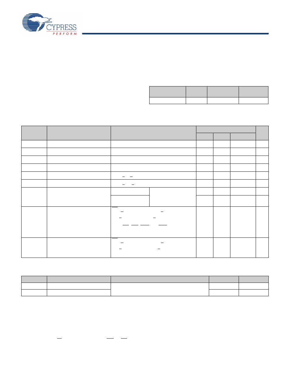
Maximum Ratings
Exceeding the maximum ratings may impair the useful life of the
device. These user guidelines are not tested.
Storage Temperature ................................ –65°C to + 150°C
Ambient Temperature with
Power Applied ........................................... –55°C to + 125°C
Supply Voltage to Ground
Potential .......................... –0.2V to 2.45V (V
CC
(max)
+ 0.2V)
DC Voltage Applied to Outputs
in High Z State
........... –0.2V to 2.45V (V
CC
(max)
+ 0.2V)
DC Input Voltage
....... –0.2V to 2.45V (V
CC
(max)
+ 0.2V)
Output Current into Outputs (LOW) ............................ 20 mA
Static Discharge Voltage........................................... >2001V
(MIL-STD-883, Method 3015)
Latch up Current...................................................... >200 mA
Operating Range
Device
Range
Ambient
Temperature
V
CC
CY62167EV18LL Industrial –40°C to +85°C 1.65V to 2.25V
Electrical Characteristics
Over the Operating Range
Parameter
Description
Test Conditions
55 ns
Unit
Min
Typ
Max
V
OH
Output HIGH Voltage
I
OH
= –0.1 mA
1.4
V
V
OL
Output LOW Voltage
I
OL
= 0.1 mA
0.2
V
V
IH
Input HIGH Voltage
V
CC
= 1.65V to 2.25V
1.4
V
CC
+ 0.2V
V
V
IL
Input LOW Voltage
V
CC
= 1.65V to 2.25V
–0.2
0.4
V
I
IX
Input Leakage Current
GND < V
I
< V
CC
–1
+1
μA
I
OZ
Output Leakage Current
GND < V
O
< V
CC
, Output Disabled
–1
+1
μA
I
CC
V
CC
Operating Supply
Current
f = f
max
= 1/t
RC
V
CC
= V
CC
(max)
I
OUT
= 0 mA
CMOS levels
25
30
mA
f = 1 MHz
2.2
4.0
mA
I
SB1
Automatic CE Power Down
Current – CMOS Inputs
CE
1
> V
CC
– 0.2V or CE
2
< 0.2V
V
IN
> V
CC
– 0.2V, V
IN
< 0.2V)
f = f
max
(Address and Data Only),
f = 0 (OE, WE, BHE and BLE),
V
CC
= V
CC
(max)
1.5
12
μA
I
SB2
Automatic CE Power Down
Current – CMOS Inputs
CE
1
> V
CC
– 0.2V or CE
2
< 0.2V,
V
IN
> V
CC
– 0.2V or V
IN
< 0.2V,
f = 0, V
CC
= V
CC(max)
1.5
12
μA
Capacitance
Tested initially and after any design or process changes that may affect these parameters.
Parameter
Description
Test Conditions
Max
Unit
C
IN
Input Capacitance
T
A
= 25°C, f = 1 MHz,
V
CC
= V
CC(typ)
10
pF
C
OUT
Output Capacitance
10
pF
Notes
6. V
IL
(min) = –2.0V for pulse durations less than 20 ns.
7. V
IH
(max) = V
CC
+ 0.75V for pulse durations less than 20 ns.
8. Full Device AC operation is based on a 100
μs ramp time from 0 to V
CC
(min) and 200
μs wait time after V
CC
stabilization.
9. Only chip enables (CE
1
and CE
2
), and byte enables (BHE and BLE) must be tied to CMOS levels to meet the I
SB2
/ I
CCDR
spec. Other inputs can be left floating.