Pin configuration, Product portfolio – Cypress CY62167EV18 User Manual
Page 2
CY62167EV18 MoBL
®
Document #: 38-05447 Rev. *G
Page 2 of 13
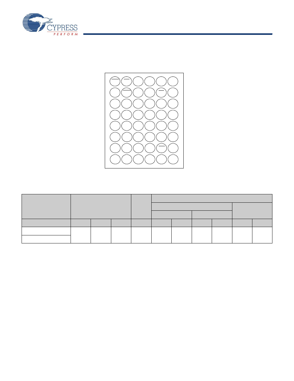
Pin Configuration
Figure 1. 48-Ball VFBGA (6 x 7 x 1mm) / (6 x 8 x 1mm) Top View
Product Portfolio
Product
V
CC
Range (V)
Speed
(ns)
Power Dissipation
Operating I
CC
(mA)
Standby I
SB2
(
μA)
f = 1 MHz
f = f
max
Min
Typ
Max
Typ
Max
Typ
Max
Typ
Max
CY62167EV18LL
1.65
1.8
2.25
55
2.2
4.0
25
30
1.5
12
CY62167EV30LL
WE
A
11
A
10
A
6
A
0
A
3
CE
1
IO
10
IO
8
IO
9
A
4
A
5
IO
11
IO
13
IO
12
IO
14
IO
15
V
SS
A
9
A
8
OE
Vss
A
7
IO
0
BHE
CE
2
A
17
A
2
A
1
BLE
V
CC
IO
2
IO
1
IO
3
IO
4
IO
5
IO
6
IO
7
A
15
A
14
A
13
A
12
A
19
A
18
NC
3
2
6
5
4
1
D
E
B
A
C
F
G
H
A
16
NC
V
cc
Notes
1. The information related to 6 x 7 x 1 mm VFBGA package is preliminary.
2. NC pins are not connected on the die.
3. Ball H6 for the VFBGA package can be used to upgrade to a 32M density.
4. Typical values are included for reference only and are not guaranteed or tested. Typical values are measured at V
CC
= V
CC(typ)
, T
A
= 25°C.
5. This part can be operated in the V
CC
range of 1.65V–2.25V at 55ns speed. It can also be operated in the V
CC
range of 2.2V–3.6V at 45ns speed.