Digilent D2XL User Manual
Page 4

Digilent D2XL Reference Manual
Digilent, Inc.
www.digilentinc.com
page 4 of 7
Copyright Digilent, Inc. All rights reserved. Other product and company names mentioned may be trademarks of their respective owners.
1
14
2
15
3
16
4
17
5
18
6
19
7
20
8
21
9
22
10
23
11
24
12
25
13
GND
Data 2 (PD2)
Data 1 (PD1)
Data 0 (PD0)
Data 3 (PD3)
Data 4 (PD4)
Data 5 (PD5)
Data 6 (PD6)
Data 7 (PD7)
Write Enable (PWE)
Interrupt (PINT)
Data Strobe (PDS)
Reset (PRST)
Address Strobe (PAS)
Wait (PWT)
CCLK
DONE
DATA IN
INIT
VDD SENSE
CABLE DET1
CABLE DET2
Decouping
three-state
buffer
GND
Vdd
DB25
connector
Program enable
switch (SW1)
JTAG
PORT
Enable
TMS
TCLK
TDI
TDO
Pull-ups on all parallel port
signals not shown
Xilinx
Spartan 2
XC2S30
TQ144
P141
P123
P140
P139
P126
P137
P130
P136
P134
P133
P132
P131
P129
P124
P142
P2
P32
P34
SPROM
Pull-ups on INIT and
DONE not shown
8-DIP
P68
P37
P39
P72
M0
M1
M2
Jumper
block
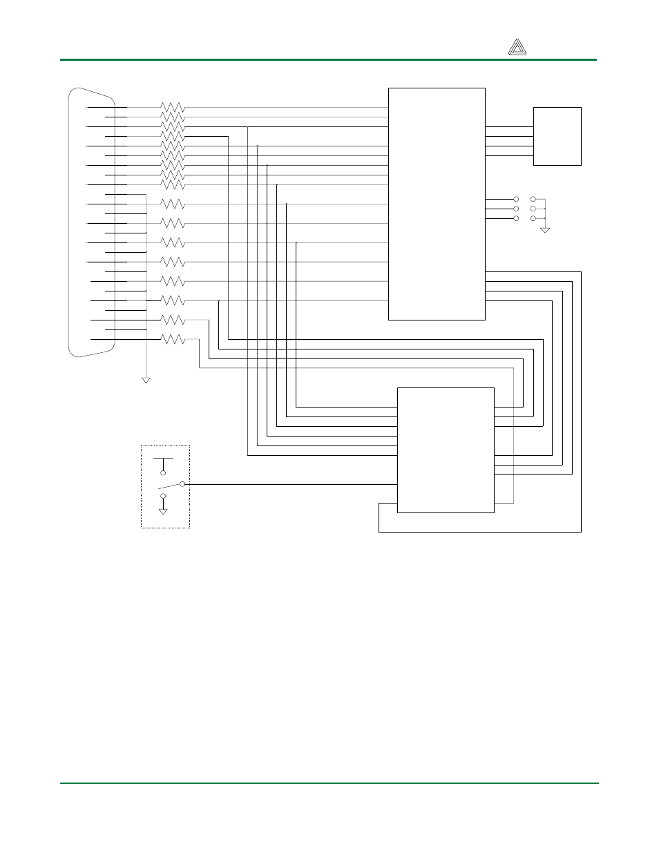
Figure 2. Parallel port and programming circuit schematic
Oscillator
The D2XL board provides a socketed half-size 8-pin DIP oscillator. The board ships with a 50MHz
oscillator, allowing for system clocks from virtually DC to 200MHz (using the Spartan 2 DLL circuit
and/or clock counter-dividers). Oscillators from 32KHz to 100MHz can easily be substituted, allowing
for a wide range of clock frequencies. The oscillator, which is connected to the FPGA GCK0 input (pin
91), is bypassed with a 0.1uF capacitor and it is located as physically close to the FPGA as possible.
