Digilent D2XL User Manual
Page 3

Digilent D2XL Reference Manual
Digilent, Inc.
www.digilentinc.com
page 3 of 7
Copyright Digilent, Inc. All rights reserved. Other product and company names mentioned may be trademarks of their respective owners.
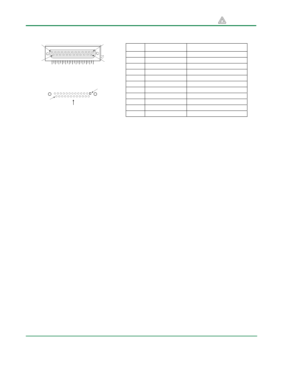
Figure 1. Parallel port connectors and signals
The D2XL board directly supports JTAG and SPROM configuration. Hardware debugger configuration
is supported indirectly. To configure the board from a computer using the JTAG mode, set switch 1
(SW1) in the JTAG position, and attach a power supply and programming cable. The power supply
must be connected before the parallel cable, or the board may hang in a non-communicating state.
The board will be auto-detected by the Xilinx JTAG programming software, and all normal JTAG
operations will be available.
To configure the FPGA from an SPROM, load the programmed SPROM into the 8-pin ROM socket
(labeled IC6), place SW1 in the PORT position, add jumpers to all mode pins, and apply power.
To configure the board using the hardware debugger protocol, a slight board modification is required –
a jumper wire must be soldered to the non-VCC side of R44. Insert wire-wrap posts into the SPROM
socket, attach the hardware debugger signals to the appropriate posts, and attach the PROG signal to
the jumper wire attached to R44. The hardware debugger programming software will now
automatically recognize the board, and hardware debugger programming can proceed as normal.
Programming circuit detail is shown below. Note that all parallel port signals are routed to the test
header J12 for easy connection of test and measurement equipment.
Pin 1
Pin 25
Top view of hole pattern, with
cable attaching from this side
Pin
EPP signal
EPP Function
1
Write Enable (O)
Low for read, High for write
2-9
Data bus (B)
Bidirectional data lines
10
Interrupt (I)
Interrupt/acknowledge input
11
Wait (I)
Bus handshake; low to ack
12
Spare
NOT CONNECTED
13
Spare
NOT CONNECTED
14
Data Strobe (O)
Low when data valid
15 Spare
NOT
CONNECTED
16
Reset (O)
Low to reset
17
Address strobe (O)
Low when address valid
18-25 GND
System
ground
Pin 13
Pin 1
Pin 14
Pin 25
DB25 parallel port connector
Front view
