Digilent 210-190P User Manual
Page 4
VmodMIB Reference Manual
www.digilentinc.com
page 4 of 5
Copyright Digilent, Inc. All rights reserved. Other product and company names mentioned may be trademarks of their respective owners.
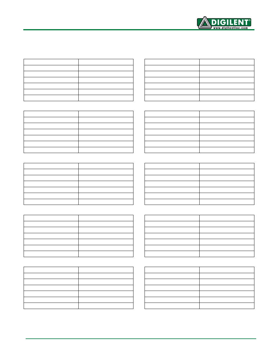
Table 2: Pmod Connector Pin Layouts
JA Top Set of Pins
Pin
Pinout
1
JA-D0_N
2
JA-D0_P
3
JA-D2_N
4
JA-D2_P
5
GND
6
VCCB
JB Top Set of Pins
Pin
Pinout
1
JB-D0_N
2
JB-D0_P
3
JB-D2_N
4
JB-D2_P
5
GND
6
VCCB
JC Top Set of Pins
Pin
Pinout
1
JC-D0_N
2
JC-D0_P
3
JC-D2_N
4
JC-D2_P
5
GND
6
VCCB
JD Top Set of Pins
Pin
Pinout
1
JD-D0_N
2
JD-D0_P
3
JD-D2_N
4
JD-D2_P
5
GND
6
VCCB
JE Top Set of Pins
Pin
Pinout
1
JE1/SDA
2
JE2/SCL
3
JE3
4
JE4
5
GND
6
VCCB
NOTE: All signals are connected via a 50 ohm resistor with
the exception of the VCCB and GND signals.
JA Bottom Set of Pins
Pin
Pinout
7
JA-CLK_N
8
JA-CLK_P
9
JA-D1_N
10
JA-D1_P
11
GND
12
VCCB
JB Bottom Set of Pins
Pin
Pinout
7
JB-CLK_N
8
JB-CLK_P
9
JB-D1_N
10
JB-D1_P
11
GND
12
VCCB
JC Bottom Set of Pins
Pin
Pinout
7
JC-CLK_N
8
JC-CLK_P
9
JC-D1_N
10
JC-D1_P
11
GND
12
VCCB
JD Bottom Set of Pins
Pin
Pinout
7
JD-CLK_N
8
JD-CLK_P
9
JD-D1_N
10
JD-D1_P
11
GND
12
VCCB
JE Bottom Set of Pins
Pin
Pinout
1
JE7
2
JE8
3
JE9
4
JE10
5
GND
6
VCCB