Absolute maximum ratings, Dc operating characteristics, Ac operating characteristics – Digilent 410-249P-KIT User Manual
Page 5
JTAG-HS2™ Programming Cable for Xilinx® FPGAs
Copyright Digilent, Inc. All rights reserved.
Other product and company names mentioned may be trademarks of their respective owners.
Page 5 of 6
Absolute Maximum Ratings
Symbol
Parameter
Condition
Min
Max
Unit
VDD (VREF)
I/O reference/supply voltage
-0.5
6
V
VIO
Signal Voltage
-0.5
6
V
I
IK
,I
OK
TMS, TCK, TDI, TDO
DC Input/Output Diode Current
VIO < -0.5V
-50
mA
VIO > 6V
+20
I
OUT
DC Output Current
±50
mA
T
STG
Storage Temperature
-20
+120
ºC
ESD
Human Body Model JESD22-A114
4000
V
Charge Device Model JESD22-C101
2000
V
DC Operating Characteristics
Symbol
Parameter
Min
Typ
Max
Unit
VDD (VREF)
I/O reference/supply voltage
1.65
2.5/3.3
5.5
Volts
TDO
Input High Voltage (V
IH
)
1.62
5.5
Volts
Input Low Voltage (V
IL
)
0
0.65
Volts
TMS, TCK, TDI
Output High (V
OH
)
0.85 x Vdd
0.95 x Vdd
Vdd
Volts
Output Low (V
OL
)
0
0.05 x Vdd
0.15 x Vdd
Volts
AC Operating Characteristics
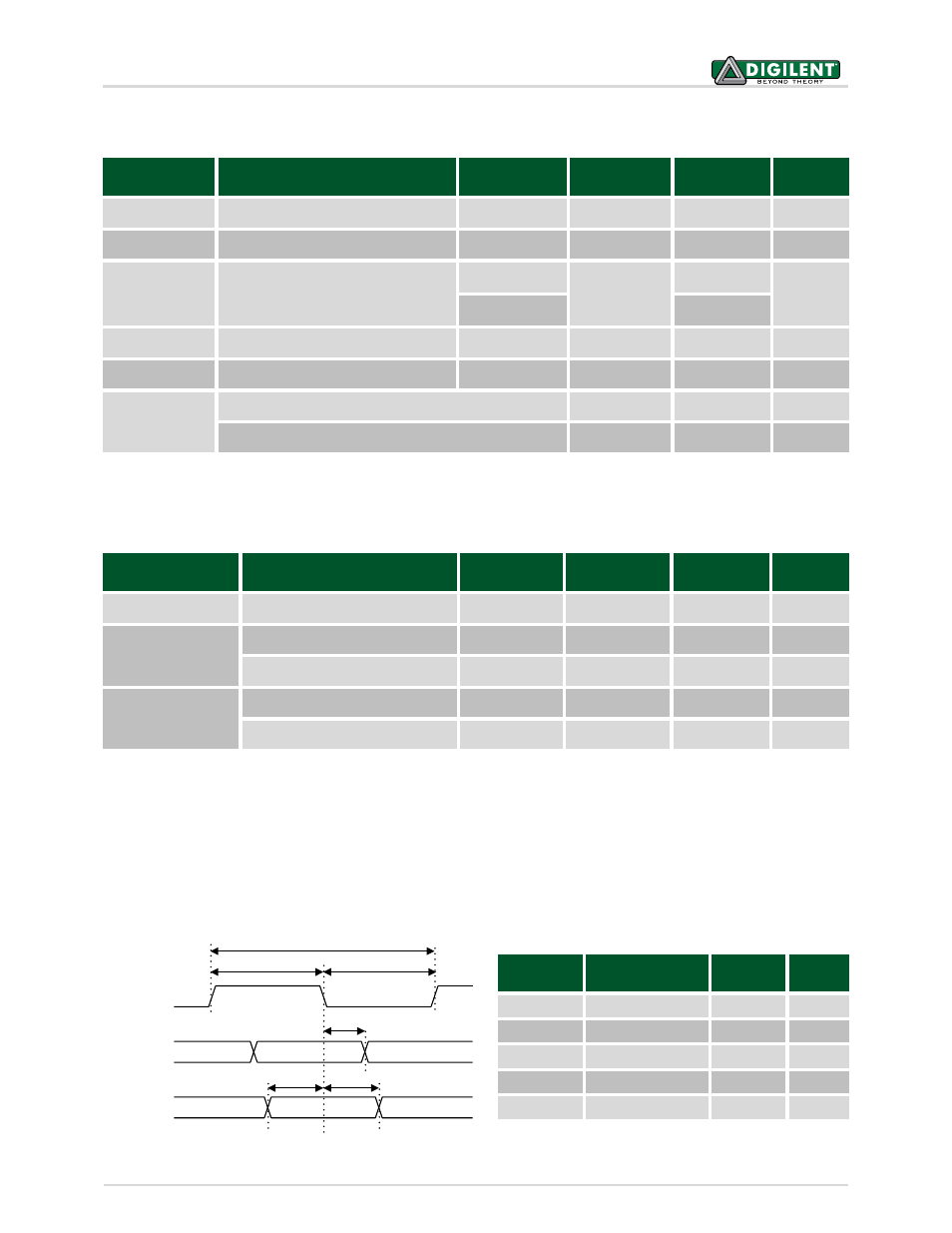
The JTAG-HS2 JTAG signals and SPI operate according to the timing diagram in Fig. 6. The HS2 supports TCK
frequencies from 30 MHz to 8 KHz at integer divisions of 30 MHz from 1 to 3750. Common frequencies include 30
MHz, 15 MHz, 10 MHz, 7.5 MHz, and 6 MHz (see Table 2).
Symbol
Parameter
Min
Max
T
CK
T
CK
period
33.3ns
125µs
T
CKH
, T
CKL
T
CLK
pulse width
16.6ns
62.5µs
T
CD
T
CLK
to TMS, TDI
0
15ns
T
SU
TDO Setup time
19ns
T
HD
TDO Hold time
0
TMS/TDI
TCK
TDO
T
CKL
T
CKH
T
CK
T
CD
T
SU
T
HD
Figure 6. Timing diagram.
Table 2.Common frequencies.