Digilent 410-249P-KIT User Manual
Page 2
JTAG-HS2™ Programming Cable for Xilinx® FPGAs
Copyright Digilent, Inc. All rights reserved.
Other product and company names mentioned may be trademarks of their respective owners.
Page 2 of 6
In addition to supporting JTAG, the JTAG-HS2 also features two highly configurable serial peripheral interface (SPI)
ports that allow communication with virtually any SPI peripheral. Both SPI ports share the same pins and only one
port may be enabled at any given time (see Fig. 3). Table 1 summarizes the features supported by each port. The
HS2 supports SPI modes 0, 1, 2, and 3.
V
IO
: 5V to 1.8V
USB2
Port
TMS
TDI
TDO
TCK
SS
MOSI
MISO
SCK
SPI Device
JTAG-HS2
GND
VDD (VREF)
GND
VIO
Port
Number
SPI Mode
Shift
LSB
First
Shift
MSB
First
Selectable
SCK
Frequency
Max SCK
Frequency
Min SCK
Frequency
Inter-byte
Delay
0
0
Yes
Yes
Yes
30 MHz
8 KHz
0 – 1000 µS
2
Yes
Yes
Yes
30 MHz
8 KHz
0 – 1000 µS
1
0
Yes
Yes
Yes
2.066 MHz
485 KHz
0 – 1000 µS
1
Yes
Yes
Yes
2.066 MHz
485 KHz
0 – 1000 µS
2
Yes
Yes
Yes
2.066 MHz
485 KHz
0 – 1000 µS
3
Yes
Yes
Yes
2.066 MHz
485 KHz
0 – 1000 µS
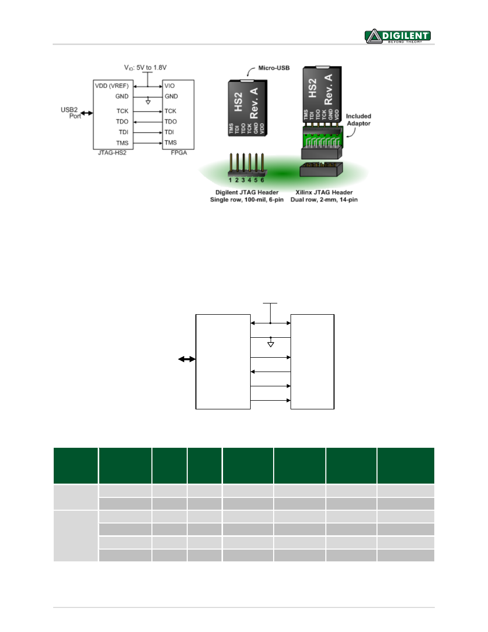
Figure 1. Diagram of signal voltages and connections.
Figure 3. JTAG-HS2 SPI Device Connections.
Figure 2. Xilinx JTAG headers.
Table 1. Features supported by each port.