Toshiba FS-160 SERIES User Manual
Page 41
Attention! The text in this document has been recognized automatically. To view the original document, you can use the "Original mode".
+5VSW
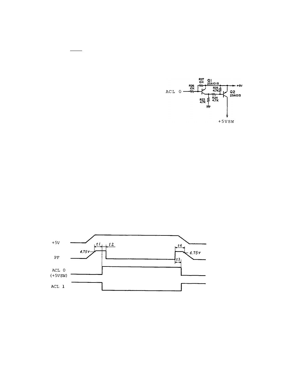
The +5VSW circuit receives the
ACLO signal as an input as
shown in Fig, 5.8, VJhen ACLO
goes high, it outputs 5V.
The output is connected to the
pull-up resistor for each out
put port of the CPU and PRC.
The reason why this circuit is
required is described below.
When ACLO is at the low level
(the CPU and PRC are reset),
the output ports of the CPU and
PRC become unstable. So this
circuit stops application of
+5V while the CPU and PRC are
reset, to prevent malfunction
of the ROM, RAM and printer
due to transmission of unneces
sary signals.
The timing and voltage values of the above outputs are shown in
Fig, 5,9 and Table 5,1, respectively.
Fig. 5.8
+5VSW Circuit
AC IN
Pig, 5,9 PS Timing Chart
tl i Sms
t2 ^ 0ms
t3 £ 40ms
t4 *
—— 2.
2
t3 "
{t4=400ms=TYP)
-24-
- MA-215 (56 pages)
- MA-156-1 (50 pages)
- TEC MA-1040-100 Series (48 pages)
- TEC MA-227 (94 pages)
- POS Terminal ST-A20 SERIES (26 pages)
- TEC MA-1400 (96 pages)
- TEC FDS-50 (104 pages)
- MA-141-100 SERIES (64 pages)
- MA-1190-100 SERIES (98 pages)
- MA-216 (84 pages)
- TEC MA-1100-100 SERIES (136 pages)
- MA-191-100 (72 pages)
- MA-1595-1 Series (218 pages)
- TEC MA-1700A-100 (158 pages)
- MA-120 Series (19 pages)
- MA-516-100 (166 pages)
- MMU-AP0091MH (117 pages)
- TEC MA-1040-400 Series (64 pages)
- TEC OM-3700 (134 pages)
- MA-1050 (96 pages)
- MA-136 (76 pages)
- MA-205-10 Series (41 pages)
- TEC MA-186-100 SERIES (119 pages)
- TEC MA-230-100 SERIES (56 pages)
- TEC EO1-11095 (152 pages)
- TEC MA-206-100 SERIES (78 pages)
- TEC MA-305 (128 pages)
- TEC MA-71 (55 pages)
- TEC MA-1350-1 (114 pages)
- TEC FS-1450-1 SERIES (144 pages)
- MA-68 SERIES (36 pages)
- TEC MA-1100-400 SERIES (138 pages)
- TEC MA-85 (120 pages)
- MA-290 (84 pages)
- TEC FDS-30 (142 pages)
- FS-2600-1 (210 pages)
- TEC MA-1300-100 (98 pages)
- FS-1650-4 SERIES (206 pages)
- TEC MA-1900 (40 pages)
- MMU-AP0071MH (32 pages)
- MA-1595-1 (263 pages)
- TEC MA-1600 (157 pages)
- MA-55 (48 pages)
- TEC MA-1060 (118 pages)